Advanced Rigid-Flex PCB Manufacturing Capabilities | SAYFU
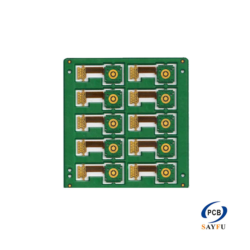
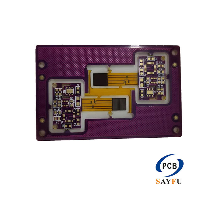
When your design demands both mechanical stability and dynamic flexibility, rigid-flex PCBs become the optimal solution.
By integrating rigid boards with flexible circuits, SAYFU Group delivers high-reliability interconnect solutions for Aerospace, Medical, and Military applications where space, weight, and durability are critical.
Whether you require a simple 4-layer rigid-flex PCB for wearable electronics or a complex 18-layer HDI rigid-flex board for avionics systems, our advanced manufacturing capabilities ensure precise impedance control, robust plated through-holes (PTH), and long-term reliability. We work exclusively with top-tier materials from DuPont, Panasonic, and other certified suppliers to guarantee performance in dynamic flex environments.
| Product Features | Standard | Advanced |
|---|---|---|
| Min Layer count | 1 | 1 |
| Max Layer Count | 14 | 18 |
| Min Board Thickness (inches) | .004”Flex / .005”Rigid | .002”Flex / .004”+ Rigid |
| Max Board Thickness (inches) | .020”Flex / .093”Rigid | .030”Flex / .200”Rigid |
| Min Core Thickness (inches) | .001”Flex / .002”Rigid | .0005”Flex / .002”Rigid |
| Min Dielectric (inches) | .001”Flex / .002”Rigid | .0005”Flex / .002”Rigid |
| Min. Starting Copper Weight | 9 μm (~.35 mil) | 5 μm (~.19 mil) |
| Max. Finished Copper Thickness (O/L) | 6 oz | >6 oz |
| Max. Finished Copper Thickness (I/L) | 6 oz | >6 oz |
| Maximum Panel Size (inches) | 12″x18″ | 12″x18” |
| Minimum Panel Size (inches) | 12″x18″ | 12″x18″ |
| Smallest Mech Drill Diameter | 100 μm (~3.9 mils) | 100 μm (~3.9 mils) |
| Min Finished Hole Size | 50 μm (~1.9 mils) | 50 μm (~1.9 mils) |
| Max Thru Hole Aspect Ratio | 16:01 | 16:01 |
| Max Blind Via Aspect Ratio | .75:1 | 1.2:1 |
| Blind Via Finished Hole Size | 50 μm/plated shut | 50 μm/plated shut |
| Buried Via Finished Hole Size | 50 μm (~1.9 mils) | 50 μm (~1.9 mils) |
| Min Line Width / Line Space (microns) | 25 μm (~.9 mil) | 20 μm (~.78 mil) |
| Min Pad Size for test | 75 μm (~2.9 mils) | 75 μm (~2.9 mils) |
| Process Pad Diameter / Mech. Drill | D + .010″ (1 mil annular ring) | D + .007″ (Tangency) |
| Stacked μm vias | Yes / copper filled | Yes / copper filled |
| Minimum Wire Bond Pad size | 75 μm (~2.9 mils) | 75 μm (~2.9 mils) |
| Controlled Impedance Tolerance | 10% | 5% |
| Solder Mask Registration | 50 μm LPI / 25 μm LDI | 25 μm LDI |
| Solder Mask Feature Tolerance | 25 μm (~.9 mil) | 25 μm (~.9 mil) |
| Solder Mask Min Dam Size | 75 μm (~2.9 mils) | 50 μm (~1.9 mils) |
| Min. Diameter Rout Cutter Available | .024″ | .018″ |
| Routed Part Size Tolerance | .005″ | .005″ |
| Laser hole location Tolerance | 12 μm (~.47 mil) | 12 μm (~.47 mil) |
| Laser Routed Part Size Tolerance | 25 μm (~.9 mil) | 25 μm (~.9 mil) |
| Thickness Tolerance | 10% | <10% |
| Sequential Lam | up to 4 cycles | up to 5 cycles |
| Buried Vias | up to 4 cycles | up to 5 cycles |
| Micro vias | Yes | Yes |
| Conductive Filled Vias | Cu filled μm vias / CB100 / Tatsuta | Cu filled μm vias / CB100 / Tatsuta |
| Non-Conductive Filled Vias | San-Ei / Peters | San-Ei / Peters |
| Surface Finishes | ||
| ENIG | Yes | Yes |
| ENIPIG | Yes | Yes |
| Wire Bondable Gold | Yes | Yes |
| Selective Gold | Yes | Yes |
| Gold over Copper | Yes | Yes |
| Immersion Silver | Yes | Yes |
| HASL / Lead free HASL | Yes | Yes |
| Selective Copper Plating | Yes | Yes |
| Fabrication | ||
| Routed Array | Yes | Yes |
| Laser Routing | Yes | Yes |
| Mech. High Precision Routing | X-Ray Pluritec System | X-Ray Pluritec System |
| Route-edge tolerance | 100 μm Laser | 75 μm Laser |
| Route-positional tolerance | 50 μm Laser | 50 μm Laser |
| Route-edge tolerance | 125 μm Mech X-Ray sys | 125 μm Mech X-Ray sys |
| Route-positional tolerance | 50 μm Mech X-Ray sys | 50 μm Mech X-Ray sus |
| Controlled depth milling | Yes | Yes |
| Edge Plating | Yes | Yes |
| Electrical Test | ||
| Flying Probe | Yes | Yes |
| Hi Pot | Yes | Yes |
| Laminate Materials | ||
| Nelco (All series) | Yes | Yes |
| Isola (FR408, 370HR, FR06, ) | Yes | Yes |
| Arlon (All series) | Yes | Yes |
| Hitachi | Yes | Yes |
| Rogers (All 3000 and 4000 series) | Yes | Yes |
Key Material Partners
We strictly use certified materials from Rogers, Isola, DuPont (Pyralux), and Panasonic to prevent delamination, improve flex life, and maintain signal integrity in complex rigid-flex structures.
Key Manufacturing Technologies
Our rigid-flex PCB production specializes in Blind & Buried Vias, Laser Drilling, and Controlled Impedance fabrication.
We support surface finishes including ENIG, OSP, and Immersion Silver, ensuring compatibility with high-reliability and fine-pitch assembly requirements.
Call to Action
Rigid-flex PCB projects often fail at the design stage, not in fabrication.
Send your Gerber files to our CAM engineers today for a free DfM review and manufacturing feasibility check.