Equipment
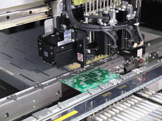
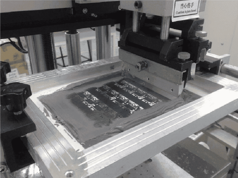
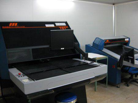
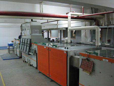
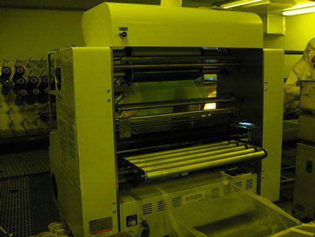
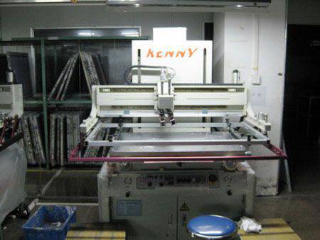
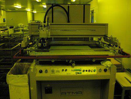
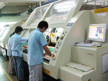
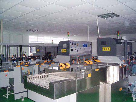
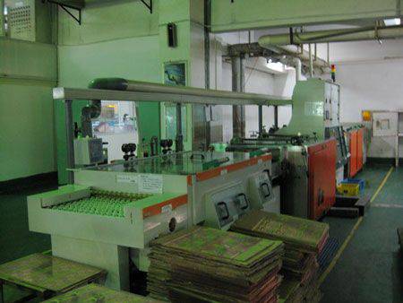
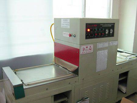
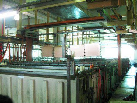
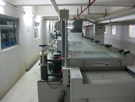
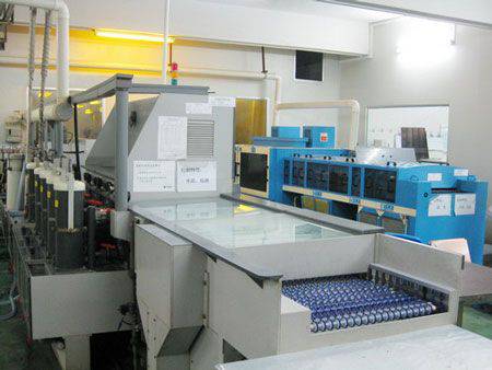
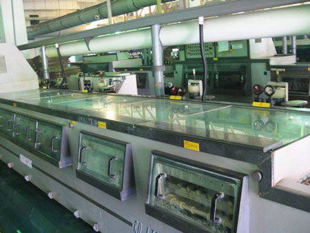
Advanced Equipment for Precision PCB Manufacturing
Advanced manufacturing equipment plays a critical role in producing reliable PCBs with fine features, complex layer structures, and consistent electrical performance. At SAYFU, our production and inspection equipment supports a broad range of PCB technologies, including HDI PCBs, high-layer-count multilayer PCBs, PTH PCBs, double-sided PCBs, FPCs, rigid-flex PCBs, IC substrates, and heavy copper PCBs.
Laser drilling and Laser Direct Imaging systems enable the accurate formation of microvias, fine traces, and tight spacing required for HDI boards, IC substrates, and high-density component layouts. High-precision exposure, etching, and registration equipment helps maintain alignment across multiple layers while supporting controlled impedance and complex routing requirements.
For multilayer, flexible, rigid-flex, and heavy copper products, advanced lamination, drilling, plating, and copper deposition equipment helps ensure reliable layer bonding, uniform hole-wall copper, and stable board structures. Process parameters are controlled according to the material, copper thickness, layer count, and end-use requirements of each project.
Automated Optical Inspection, electrical testing, impedance testing, and other inspection systems are used throughout production to identify defects and verify that finished boards meet customer specifications. Together with standardized process control, these capabilities allow SAYFU to support PCB projects from prototypes and engineering samples to stable volume production.
We continue to invest in manufacturing and inspection technology to meet the growing requirements of applications in medical electronics, aerospace, industrial control, communications, automotive electronics, and advanced consumer devices.