SAYFU manufactures rigid, multilayer, HDI, flexible and rigid-flex PCBs for prototype, NPI and volume production programs. Use this page to compare standard, advanced and engineering-review capability levels before submitting your design for quotation.
| Up to 30 Layers | Min. 3/3 mil Trace/Space | Min. 0.10 mm Drill | 1/3 oz – 4 oz Copper | ±10% Impedance |
PCB Manufacturing Capabilities at a Glance
Bare PCB manufacturability cannot be determined from a single parameter. Final capability depends on board type, layer count, material, copper weight, via structure, impedance requirements and production stage — and how these factors interact in the complete design.
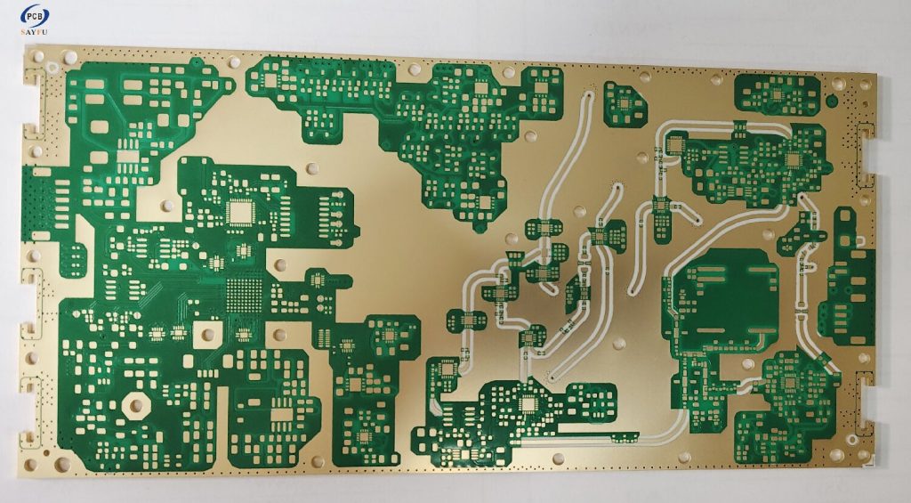
Rigid PCB Standard multilayer rigid PCB from 1 to 30 layers. FR-4, high-Tg FR-4, halogen-free, Rogers, Taconic and Arlon materials. Up to 533 × 1,219 mm. → Rigid PCB
HDI PCB Blind and buried vias, laser microvias, sequential lamination. 1+N+1 and 2+N+2 in production; 3+N+3 for selected prototypes. Up to 20 layers in production, up to 30 layers for samples. → HDI PCB
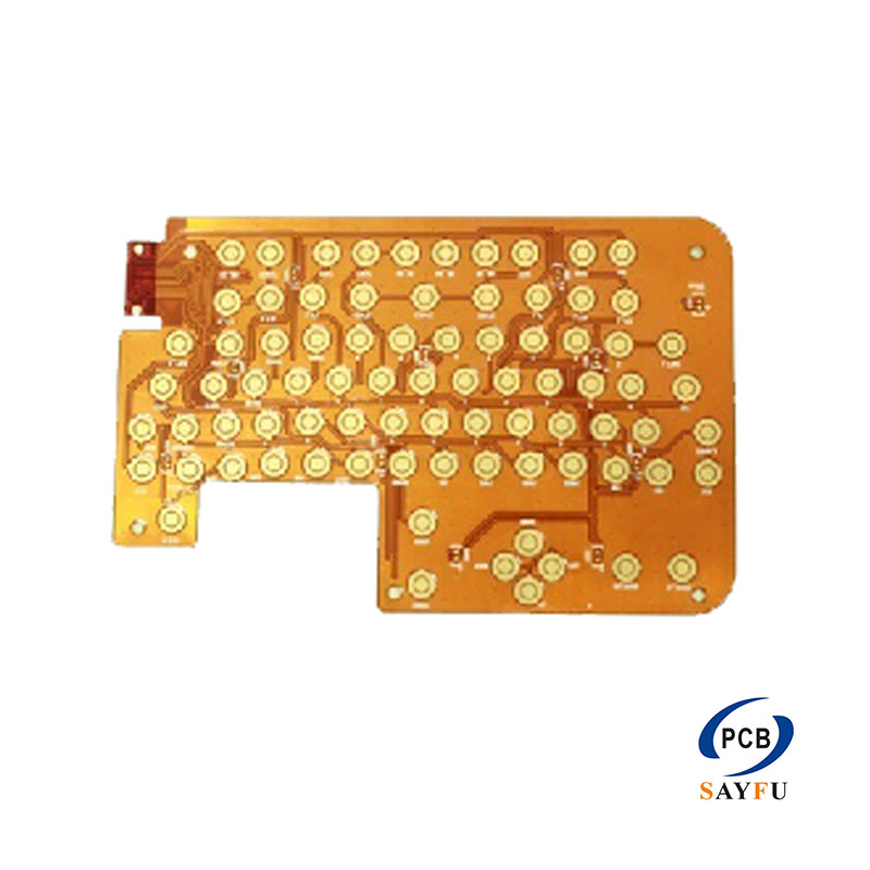
Flex PCB Polyimide base, adhesive and adhesiveless construction, coverlay and stiffener. 1–6 layers; standard production 1–4 layers. Static and dynamic bend applications. → Flex PCB
Rigid-Flex PCB Combined rigid and flexible zones in a single construction. Up to 14 layers standard, 18 layers advanced. Up to 5 sequential lamination cycles. → Rigid-Flex PCB
High-Frequency PCB Rogers, Taconic, Arlon and ceramic-filled laminates for RF and microwave applications. Controlled impedance and mixed-material stack-up reviewed on submission. → High Frequency PCB
Heavy Copper PCB High-current and thermal power applications within the verified rigid PCB copper range. Designs above 4 oz or combining heavy copper with fine spacing require engineering review. → Heavy Copper PCB
Capability Level Legend
| Level | Meaning |
|---|---|
| Standard | Stable range for typical production |
| Advanced | Supported under defined conditions and confirmed stack-up |
| Engineering Review Required | Requires complete file review before commitment |
SAYFU supports projects from engineering sample through prototype, NPI, low-volume and volume production. Production stage affects which capability levels are available — some advanced limits are accessible for prototype builds but require process validation before stable volume production.
PCB Manufacturing Specifications
The four tables below cover construction, copper and drilling, via structures, and surface finishes. Each row shows the capability range, the applicable level, and the conditions that determine the final result.
One condition applies across all tables: published limits represent individual parameters. Combining multiple extreme values in one design — minimum trace, maximum copper, high layer count, thin board, specialty material — requires engineering review before production is confirmed.
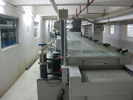
Table A: Construction and Materials
| Parameter | Capability | Level | Key Conditions |
|---|---|---|---|
| Layer Count | 1–30 layers | Standard / Advanced | Material, thickness and copper weight dependent |
| Board Thickness | 0.4–6.0 mm | Standard / Advanced | Layer count, copper and aspect ratio dependent |
| Maximum Board Size | 533 × 1,219 mm | Advanced | Surface finish and panel handling dependent |
| Materials — Standard | FR-4, High-Tg FR-4, Halogen-free FR-4 | Standard | Availability and lead time dependent |
| Materials — Advanced | Rogers, Taconic, Arlon, ceramic-filled laminates, polyimide | Advanced | Stack-up and impedance review required |
| Mixed-Material Stack-up | Available | Engineering Review | Full stack-up and impedance data required |
| IPC Quality Class | Class 2 and Class 3 | Project-specific | Acceptance criteria to be confirmed |
Table B: Copper, Trace and Drilling
| Parameter | Capability | Level | Key Conditions |
|---|---|---|---|
| Copper Weight | 1/3 oz – 4 oz | Standard / Advanced | Fine lines depend on finished copper thickness |
| Minimum Trace / Space (Rigid) | Down to 3/3 mil | Advanced | Finished copper thickness and layer position |
| Minimum Trace / Space (HDI — Production) | 75/75 μm outer; 75/75 μm inner | Advanced | Copper weight dependent |
| Minimum Trace / Space (HDI — Sample) | 50/75 μm outer; 50/50 μm inner | Engineering Review | Sample-only; not representative of volume capability |
| Minimum Trace / Space (Flex) | Down to 3/3 mil | Advanced | Finished copper dependent |
| Minimum Mechanical Drill | 0.10 mm finished | Advanced | Board thickness and aspect ratio dependent |
| Through-Hole Aspect Ratio | Up to 12:1 | Advanced | Hole size and board thickness dependent |
| Minimum BGA Pitch | 0.30 mm | Advanced | Pad, mask and assembly review required |
| Minimum BGA Pad | 0.20 mm | Advanced | Design review required |
| Profile Tolerance | ±0.10 mm routing | Standard | Geometry dependent |
Table C: Via Structures and HDI
| Parameter | Capability | Level | Key Conditions |
|---|---|---|---|
| HDI Structure — Production | 1+N+1, 2+N+2 | Advanced | Sequential lamination required |
| HDI Structure — Sample | 3+N+3 | Engineering Review | Not representative of volume production capability |
| Layer Count — HDI Production | 1–20 layers | Advanced | Construction dependent |
| Layer Count — HDI Sample | 22–30 layers | Engineering Review | Engineering review before commitment |
| Laser Microvia / Land | 75/200 μm | Advanced | Dielectric thickness and pad design dependent |
| Maximum Laser Hole | 250 μm | Advanced | Process dependent |
| Minimum SBU Dielectric | 38 μm production / 30 μm sample | Advanced / Engineering Review | Material dependent |
| Blind Vias | Supported | Advanced | Layer span and structure to be confirmed per design |
| Buried Vias | Supported | Advanced | Sequential lamination required |
| Stacked Microvias | Supported (sample) | Engineering Review | Dielectric thickness, reliability review required |
| Staggered Microvias | Supported | Advanced | Structure dependent |
| Via-in-Pad | Supported | Advanced | Fill method to be confirmed |
| Conductive Via Fill | Supported | Advanced | Rigid-flex; dimensions and finish dependent |
| Non-Conductive Via Fill | Supported | Advanced | Rigid-flex; application dependent |
| Controlled Impedance — Rigid | ±10% | Standard | Confirmed stack-up required |
| Controlled Impedance — HDI Production | ±7% | Advanced | Stack-up and coupon required |
| Controlled Impedance — HDI Sample | ±5% | Engineering Review | Full design and material data required |
| Back Drilling | [PENDING] | [PENDING] | Confirm capability and residual stub tolerance |
Table D: Surface Finishes and Special Processes
| Finish / Process | Applicable Board Types | Level |
|---|---|---|
| Lead-Free HASL | Rigid, HDI, Rigid-Flex | Standard |
| ENIG | Rigid, HDI, Flex, Rigid-Flex | Standard |
| OSP | Rigid, HDI | Standard |
| Immersion Silver | Rigid, HDI, Rigid-Flex | Standard |
| Immersion Tin | Rigid, HDI | Standard |
| Hard Gold | Rigid | Advanced |
| Soft Gold | Rigid | Advanced |
| ENEPIG / ENIPIG | Rigid, Rigid-Flex | Advanced |
| Gold Fingers | HDI | Advanced |
| Selective Hard Gold | HDI | Advanced |
| Wire-Bondable Gold | Rigid-Flex | Advanced |
| Selective Gold | Rigid-Flex | Advanced |
| Edge Plating | Rigid-Flex | Advanced |
| Controlled-Depth Milling | Rigid-Flex | Advanced |
| Laser Routing | Rigid-Flex | Advanced |
| Flying Probe Test | Rigid, Rigid-Flex | Standard |
| Dedicated Test Fixture | Rigid | Standard |
| Hi-Pot Test | Rigid-Flex | Project-specific |
Surface finish availability depends on board type, material and end-use requirements. Not every finish listed applies to every board construction — confirm during engineering review.
Advanced Capabilities and Engineering Review Triggers
Most designs fall within the standard or advanced ranges shown above. The table below identifies the specific conditions that move a design from the advanced range into engineering review territory — not because SAYFU cannot manufacture it, but because the combination of parameters requires confirmation before production is committed.
| Capability | What SAYFU Supports | Engineering Review Is Required When |
|---|---|---|
| HDI and Microvias | 1+N+1, 2+N+2 production; 3+N+3 samples; 75/200 μm laser via/land | 3+N+3 structure; stacked microvias; dielectric < 38 μm; laser via filling; 50/50 μm inner routing |
| Controlled Impedance | ±10% rigid; ±7% HDI production; ±5% HDI sample | Tolerance tighter than ±7%; mixed-material stack-up; impedance through flex zones |
| Flex PCB | 1–6 layers; 3/3 mil; 0.10 mm laser hole | 5–6 layers; dynamic bend application; tight bend radius; heavy copper on flex layers |
| Rigid-Flex PCB | Up to 14 layers standard / 18 layers advanced; 4–5 lamination cycles | Dynamic bend zones; HDI rigid-flex combination; high layer count with tight impedance |
| Heavy Copper | Verified rigid range up to 4 oz | Above 4 oz; fine spacing alongside heavy copper; multiple heavy-copper inner layers |
| Large-Format Rigid | Up to 533 × 1,219 mm | Panel handling, surface finish compatibility and registration across format |
| Via Filling | Conductive and non-conductive fill | Via dimensions, finish compatibility, quantity and reliability class |
| Special Routing | Laser routing, controlled-depth milling, edge plating | Tight positional or depth tolerance; geometry requiring pre-submission review |
A design may satisfy several published individual values and still require engineering review when those values are combined in one construction. This is not an exception — it is the standard rule for complex PCB design.
Engineering Review and Bare Board Testing
What We Check Before Production
When a complete file set is submitted, SAYFU’s engineering team reviews the design for manufacturing compatibility before production starts. The review covers:
- Gerber / ODB++ / IPC-2581 file completeness and layer assignment
- NC Drill and fabrication drawing consistency
- Layer stack-up, material and copper thickness
- Trace / space against copper weight and layer position
- Minimum drill size against board thickness and aspect ratio
- Drill-to-copper and copper-to-edge spacing
- Annular ring and via structure
- Controlled impedance — target, trace reference and stack-up
- Blind, buried and microvia layer spans
- Via fill and cap requirements
- Solder mask dam
- Surface finish compatibility
- Special mechanical features — slots, castellations, countersink, edge plating
- Conflicts between combined extreme parameters
Following review, the engineering team returns engineering questions, DFM findings, stack-up recommendations, material alternatives where required, and production or lead-time confirmation. Any proposed material substitution is submitted for customer approval — no substitution is made without explicit confirmation.
Initial EQ and DFM feedback is returned within 1–2 working days of receiving a complete file set.
Not Sure Whether Your PCB Fits Our Standard Capabilities?
Submit your Gerber or ODB++ files, NC Drill, stack-up, fabrication drawing, quantity and critical process requirements. SAYFU’s engineering team will review the complete construction and confirm whether the design falls within standard capability, advanced capability, or requires additional process evaluation.