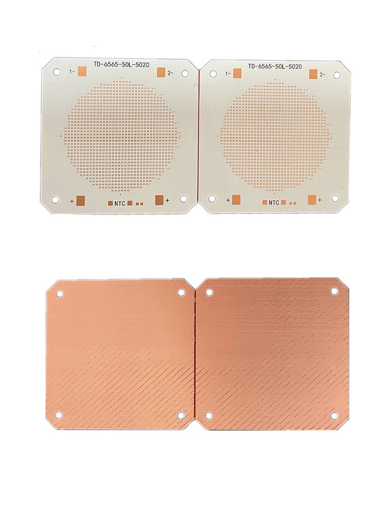
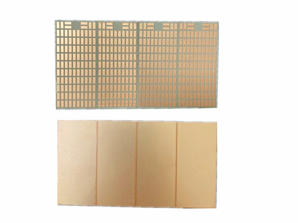
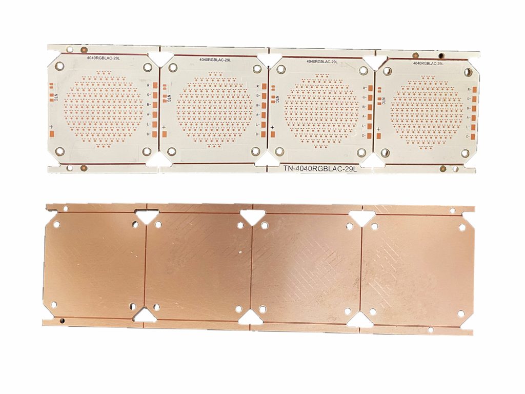
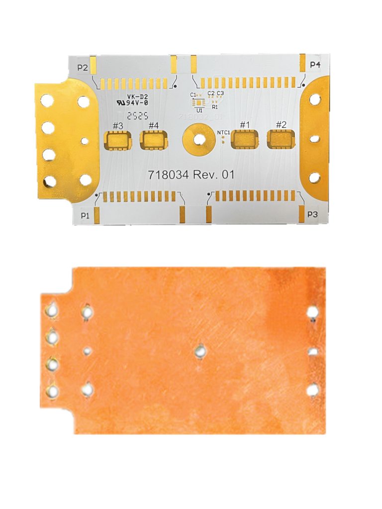
Copper Core PCB is wildly used in many fields, is an very important branch of printed circuit board. Belew are some pictures of copper based printed circuit boards:
In this artical we will introduce such PCB from below 3 parts:
Part 2 The Fabrication Procedures of Copper-clad PCB
Part 3 The Optimization Methods for Copper Based PCB Heat Dissipation Ability
Part 1 Basic Concepts
Simply speaking, Copper core PCB is a type of metal-based laminate with copper as the base material, with excellent heat dissipation performance.
1. Definition and Composition of Copper Core PCB
Copper based PCB is a special metal-based PCB, which uses copper metal as the base material and combines the copper substrate with a conductive layer (usually copper foil) through an insulating layer. There are mainly three parts:
- Copper Substrate Layer: High-purity copper plate (purity ≥ 99.9%) is used to provide excellent thermal conductivity and structural support.
- Insulating Layer: Composed of ceramic-filled polymer, so it has both electrical insulation and thermal conductivity.
- Conductive Layer: Thin copper foil (usually 1oz-3oz) is used for circuit pattern fabrication.

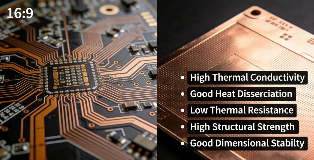
2. Copper Core PCB Main Characteristics and Advantages
Compared with traditional FR-4 PCB, copper based substrates have significant characteristics:
- High Thermal Conductivity: The thermal conductivity of Copper Heat Spreader can reach 10-400W/(m·K), which is much higher than that of FR-4 (0.3-0.5W/(m·K)).
- Good Heat Dissipation: Copper Heat Spreader can quickly conduct heat from heating element components to the heat dissipation system.
- Low Thermal Resistance: Copper Heat Spreader Reduces the transferring resistance of heat between components and heat sinks.
- High Structural Strength: The copper substrate provides better mechanical support and deformation resistance.
- Good Dimensional Stability: Low coefficient of thermal expansion, suitable for precision circuit PCB applications.
3.Copper Core PCB Typical Application Fields
With its excellent performance, Copper Core PCBs are widely used in:
– LED lighting: high-power LED modules such as street lights, spotlights, and automotive headlights
– Power electronics: inverters, power supplies, motor controllers
-Telecom equipments: RF amplifiers, base station power modules
– Automotive electronics: engine control units, vehicle power supply systems
– Consumer electronics: high-end graphics cards, CPU heat sinks, laptop cooling modules
4. Common Types and Classifications
According to different characteristics and applications, Copper-Clad Substrate PCB can be divided into:
4-1 By Insulation Layer Type:
– Epoxy glass cloth-based Copper-Clad Substrate
– Ceramic-based Copper-Clad Substrate (Al₂O₃, AlN, Si₃N₄, etc.)
– Metal-Insulator Copper-Clad Substrate(MIM)
4-2 By Thermal Conductivity:
– Ordinary thermal conductive Copper-Clad Substrate (10-50W/(m·K))
– High thermal conductive Copper-Clad Substrate(50-200W/(m·K))
– Ultra-high thermal conductive Copper-Clad Substrate (above 200W/(m·K))
5. Manufacturing Process Characteristics
The production process of Copper Core PCB differs from traditional PCBs:
- Copper Substrate Pretreatment: Surface cleaning and roughening treatment
- Insulating Layer Coating: Formation of insulating dielectric layer via roller coating or lamination
- Conductive Layer Lamination: High-temperature pressing of copper foil and insulating layer
- Circuit Fabrication: Circuit pattern fabrication using traditional PCB etching process
- Surface Treatment: Typically OSP (Organic Solderability Preservative), immersion gold, or Immersion Silver
Part 2 The Fabrication Procedures of Copper-clad PCB
The manufacturing process of copper-clad pcb is more complex than that of normal PCBs, requiring specialized technology to balance heat dissipation and electrical conductivity.
Overview of Copper-Clad PCB Manufacturing Processes
The production of copper based pcb can be divided into seven core steps, forming a complete manufacturing chain from material pre-treatment to final inspection:Material Pretreatment → Insulation Layer Preparation → Metallization → Lamination → Circuit Fabrication → Post-Processing → Quality Inspection
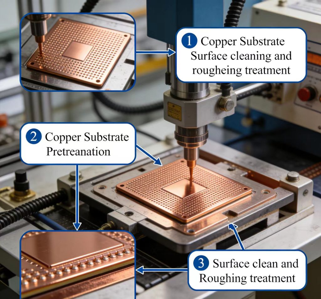
1.Copper Substrate Pretreatment of Copper Core PCB
To ensure strong adhesion in subsequent steps, the copper substrate material needs rigorous surface treatment:
1-1.Material Selection and Cutting: High-purity electrolytic copper plates (≥99.9%) are needed and will be cut into work blanks according to size requirement.
1-2.Surface Grinding: Use abrasive papers (800–1200 grit) or sandblasting to achieve a surface roughness of Ra 0.8–1.2μm.
1-3.Chemical Cleaning:
Degreasing: Alkaline cleaners remove oils.
Acid Pickling: Nitric or sulfuric acid solutions eliminate oxide layers.
Micro-Etching: Ammonium persulfate solution forms micro-concave structures.
Passivation: Chromate or silane coupling agents enhance adhesion to the insulation layer
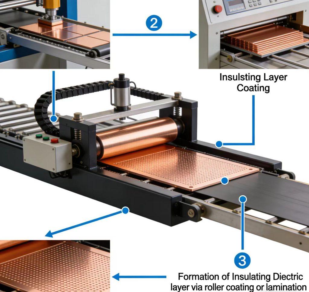
2.Insulation Layer Fabrication of Copper Core PCB
The insulation layer is the core functional part, determining thermal conductivity and insulating performance. Take Ceramic-Filled Type (Mainstream Process)as an example:
2-1 Resin Preparation: Mix epoxy/PI with curing agents.
2-2 Thermal Filler Dispersion: Add ceramic particles e.g., Al₂O₃, BN, AlN ( 1–5 μm diameter).
2-3 Viscosity Adjustment: Control slurry viscosity to 5,000–15,000 cps (25°C).
2-4 Coating Formation:
2-4-1 Blade Coating: Thickness 50–200 μm, tolerance ±5 μm.
2-4-2 Tape Casting: Suitable for mass production with better uniformity
2-5 Semi-Curing: Pre-curing at 80–120°C for 10–30 minutes to achieve B-stage state.
3、Metallization enables electrical connectivity on both sides of the insulation layer:
3-1.Laser Drilling:
3-1-1 Use UV or CO₂ laser drilling to create vias (50–200 μm diameter).
3-1-2 Plasma cleaning removes debris from via walls.
3-2.Metallization Process:
3-2-1 Electroless Copper Plating: Plating 0.5–1 μm copper to via walls and insulating layer surface.
3-2-2 Electrolytic plating: Increases copper thickness to 5–15 μm for conductivity.
3-3.Copper Foil Lamination:
3-3-1 Use 1/2–3 oz electrolytic or rolled copper foil.
3-3-2 Surface treatments (e.g., zinc/nickel plating) to prevent oxidation
4. Multilayer Lamination Technology for Copper Core PCB
All materials layers were combined firmly with high temperature and pressure.
4-1. Layer Stack up: Follow “copper base → insulation layer → copper foil” structure.
4-2.Lamination Parameters:
4-2-1Temperature: Room temperature → 120°C (preheating) → 180–220°C (curing) → cooling.
4-2-2 Pressure: 20–40 kg/cm².
4-2-3 Time: 60–120 minutes (adjusted based on thickness).
4-3. Vacuum Control: Chamber vacuum ≤50 Pa to prevent bubbles.
4-4.Post-Lamination: Cool naturally, remove edge burrs
5、 Circuit Pattern Fabrication
Copper Core PCB Circuit patterns are made similarly like normal PCB pattern transferring processes:
5-1. Dry Film:
5-1-1.Film Lamination: Apply 30–50 μm dry film at 100–120°C.
5-1-2 Exposure: UV exposure at 80–120 mJ/cm².
5-1-3 Development: Sodium carbonate solution (1.0–1.2%), 40–60 seconds.
5-2. Etching Process:
5-2-1. Acidic Etching: CuCl₂ or FeCl₃ solution, etch factor ≥3.0.
5-2-2. Line Width Control: Precision ±10 μm, minimum width/spacing of 30/30 μm.
5-3. Stripping and Cleaning: Remove residual film, neutralize acids

6. Rest Procedures of Copper Core PCB
Auxiliary treatments after circuit fabrication:
6-1. Surface Finishing:
OSP: Organic solderability preservative (0.2–0.5 μm).
ENIG: Gold layer 0.8–2.0 μm, nickel layer 5–10 μm.
Silver Plating: For high-frequency applications (1–3 μm).
6-2. Shape Processing:
CNC Routing: Positioning accuracy ±0.05 mm.
Laser Cutting: For complex shapes, stress-free.
6-3. V-CUT : 30–45° angle, residual copper thickness 0.1–0.3 mm (if needed for panel separation).
6-4. Silkscreen: UV ink markings for product identification
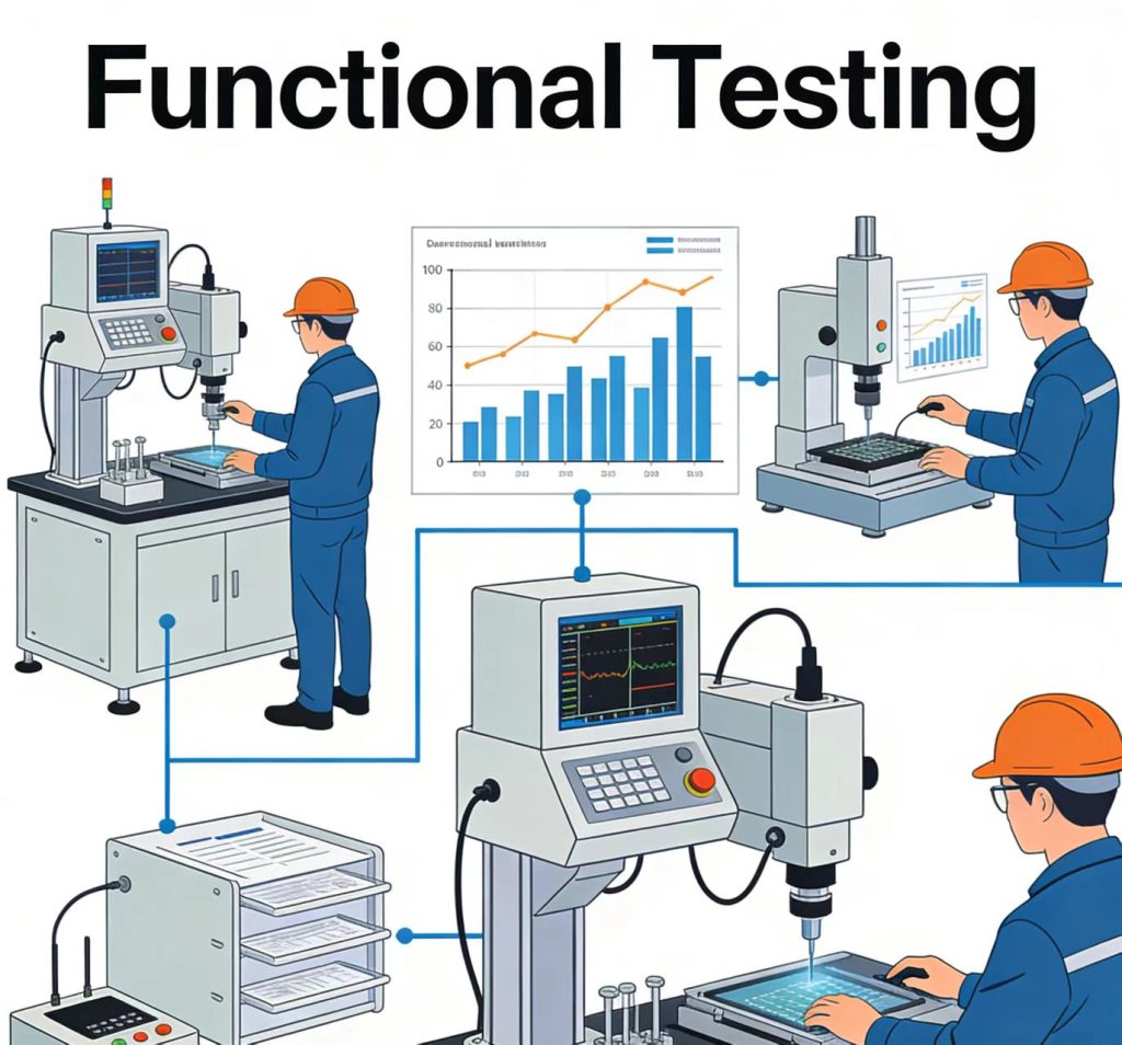
7、 FQC&Reliability Tests
FQC&Reliability Test etc comprehensive checks ensures high quality of copper core pcb products, they are listed as below:
Visual Inspection:
AOI: Detects line defects, shorts, or opens.
Microscope: Identifies bubbles, delamination, or lamination problems.
Thermal Conductivity: Measured via heat flow meter or laser flash analysis.
Insulation Resistance: ≥1×10¹⁴ Ω (500V DC).
Voltage Withstand: AC 2500V for 1 minute without breakdown.
Reliability Testing:
Thermal Shock: -40°C to 125°C, 1000 cycles.
Humidity Testing: 85°C/85% RH, 1000 hours.
Peel Strength Test: ≥1.5 N/mm (copper foil to insulation layer)
This structured process ensures copper-clad substrates meet high standards for thermal management and electrical reliability, critical in applications like LED lighting, power modules, and automotive electronics
| Process | Key Parameters | Value&Tolerance | Impact for Quality |
| Insulating Coating | Thickness | +/-5um | Thermal Conductivity |
| Lamination | Temperature Curve | 180-220 °C | Resin solidification(TG) |
| Etching | Etching Factor | >=3.0 | Line Perpendicularity |
| Surface Finish | Plating thickness | 0.8-2.0um | Solder Ability |
| FQC&Testing | Thermal Resistance Test | <=0.5°C/W | Heat Dissipation Ability |
Part 3 The Optimization Methods for Copper Based PCB Heat Dissipation Ability
With materials improvement, structural design optimization and heat dissipation system improvement, the heat dissipation rate of copper core pcb can be enhanced significantly, which is extremely important to such PCB.
A. Material System Optimization of Copper Core PCB
The foundation for the thermal performance of Copper Core PCB lies in material selection and formulation optimization, aiming to reduce thermal resistance from the source.
1.Enhancing Insulation Layer Thermal Conductivity
Upgrading High Thermal Conductivity Fillers:Traditional epoxy resins filled with Al₂O₃ (thermal conductivity ~30 W/m·K) can no longer meet high-power demands. Newly developed technology utilize fillers like boron nitride (BN, 70-200 W/m·K) or aluminum nitride (AlN, 180-320 W/m·K). With surface improved modification technology, filler loading rates can exceed 50%, enabling the insulation layer’s thermal conductivity to break through 10 W/m·K (standard 1-3 W/m·K only).
Core-shell structured fillers (e.g., Al₂O₃@BN) are used to solve brittleness problem caused by high filler loading, maintaining flexural strength above 150 MPa.
2. Resin Innovation:
- Replacing traditional epoxy resins with polyimide (PI) or cyanate ester resins maintains stable thermal performance above 200°C.
- Using graphene/carbon nanotube compositing system to form a three-dimensional thermal network, increasing the insulation layer’s thermal conductivity by 3-5 times.
- Improving Copper Substrate Performance
3-1.Application of Oxygen-Free High Conductivity (OFHC) Copper: Increasing purity from 99.9% to 99.99% can increase thermal conductivity from approximately 380 W/m·K to 401 W/m·K. It can make it suitable for extreme high power as high as 500W.
3-2. Microcrystalline Structure Control: Utilizing processes like rolling to control copper grain size between 5-10 micrometers reduces grain boundary thermal resistance and improves in-plane thermal conductivity uniformity.
B. Structural Design Innovation for Copper Core PCB
Breaking through the limitations of traditional layer structures to build efficient heat conduction paths is very important and new technology for copper core PCB. We will descripe the innovation from 3 respects as below:
1.Thermal-Electrical Separation Technology
1-1.Principle:
Physically separating the circuit pattern from the thermal conduction channels. Heat-generating components connect directly to the copper substrate via copper pillars, in this way, it can break the bottleneck of the insulation layer
1-2. Key Parameters:
Pillar diameter: 0.2-0.5mm (laser window opening accuracy up to ±10μm);
Array density: 100-200 pillars/cm² (e.g., in LED applications);
Thermal resistance reduction: Can be reduced by over 80% compared to traditional structures (from ~0.8 °C/W to below 0.15 °C/W)
Processes:
A [Substrate Cleaning] –> B[Insulation Layer Coating] –> C[Laser Ablation/Chemical Etching] –> D[Copper Pillar Plating/Thickening] –> E[Circuit Pattern Etching]
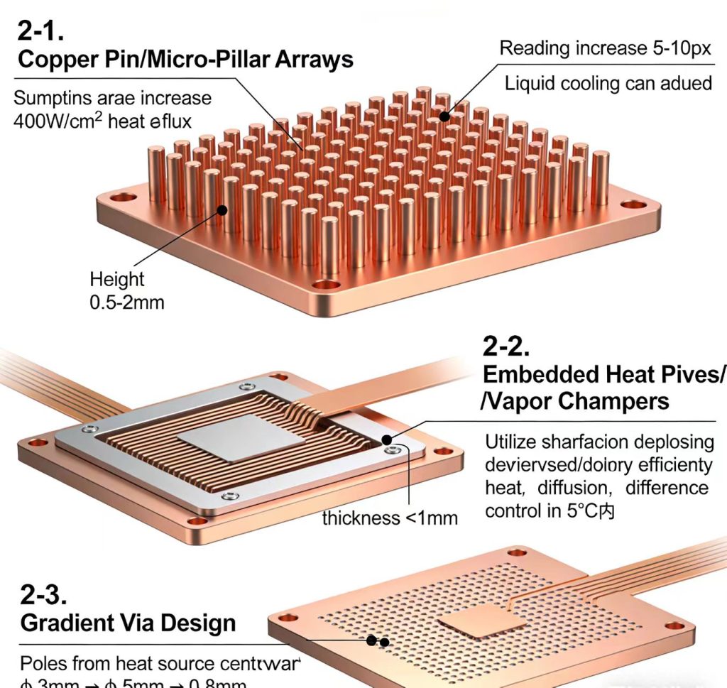
2. 3D Thermal Dissipation Structures
2-1. Copper Pin/Micro-Pillar Arrays: Forming arrays of copper pins (height 0.5-2mm) on the substrate surface can increase the dissipation area by 5-10 times. With liquid cooling, this can handle heat fluxes up to 400W/cm².
2-2. Embedded Heat Pipes/Vapor Chambers: Embedded ultra-thin heat pipes (thickness <1mm) into the CCL utilizes phase change for efficient two-dimensional heat spreading, the temperature differences can be controlled within 5°C.
2-3. Gradient Via Design: Gradient via design is being used, via diameters can be gradually changed from φ0.3mm → φ0.5mm → φ0.8mm from the heat source center outward, which optimizes the heat diffusion path.
3. Partial Reinforcement Design
3-1. Thick Copper Areas: Implementing partial thick copper (3-5 oz, compared to standard 1 oz) under power components, complemented by arrays of thermal vias (8-12 mil diameter, 30-40 mil pitch)
3-2. Embedded Copper Blocks: The copper blocks (e.g., 6mm×4mm×1mm) can be soldered directly under chips, connecting to the substrate through plated through-holes. It can reduce thermal resistance by 40%.
3-3. Solder Mask Opening (SMO): Exposing thermal pad areas increases the area for natural convection heat transfer. Combining this with thicker solder paste can reduce contact thermal resistance.
C. Manufacturing Process Optimization for Copper Core PCB
Improving the integrity of thermal paths through precision manufacturing controlling to optimize the manufacturing processes of copper based PCB.
Lamination Process Improvements
- Vacuum Control: Maintaining vacuum ≤50 Pa in the lamination chamber avoids bubbles in the insulation layer (the bubbles can increase partial thermal resistance by 300%)
- Staged Pressure Profile: from room temperature → 5 kg/cm² during preheating → 25 kg/cm² during curing → 15 kg/cm² during cooling) ensures no delamination at the interface between the insulation layer and the copper substrate.
Surface Treatment Technologies
- Lead-Free Treatment: Using Electroless Nickel Immersion Gold (ENIG) instead of traditional lead-tin plating. Gold layer thickness is typically 0.8-2μm, nickel layer 5-10μm, helping to reduce inter-facial thermal resistance.
- Micro-structured Surfaces: Using electro-chemical etching to create micro-scale pillar structures with roughness (Ra) of 1.5-2.0μm, enhancing the wett-ability of thermal interface materials
- Graphene Coating: Depositing a 50-100nm thick Graphene film on the dissipation surface can enhance radiative heat dissipation by 15-20%.
D. System-Level Thermal Integration of Copper Core PCB
For copper core PCBs, CCLs need to work together with all the thermal management system to form a complete heat dissipation path.
1. Thermal Interface Material (TIM) OptimizationThermal Gels:
Selecting high elastic gels with thermal conductivity of 3-8 W/m·K and compression rates >30% to fill interface, controlling the gaps less than 5μm. Sintered Silver Technology: Using nano-silver paste sintering between high-power devices and the CCL to form a metallic bonded interface with very low thermal resistance (<0.05 °C/W).
2.Heat-sink Design
- Integrated Heat Sinks: Using copper-aluminum composite fins (copper core for base+aluminum fins) can reduce weight by 35% and cost by 50% compared to all-copper solutions
- Directed Airflow Design: Optimizing fin orientation based on thermal simulation results, equiped with high-static-pressure fans (e.g., 4000 rpm), can increase airflow velocity to 6 m/s.
- Liquid Cooling Integration: Directly attaching micro-channel cooling plates to the CCL, flow rates controlled at 1-2 L/min, keeping the inlet-outlet temperature difference ≤8°C
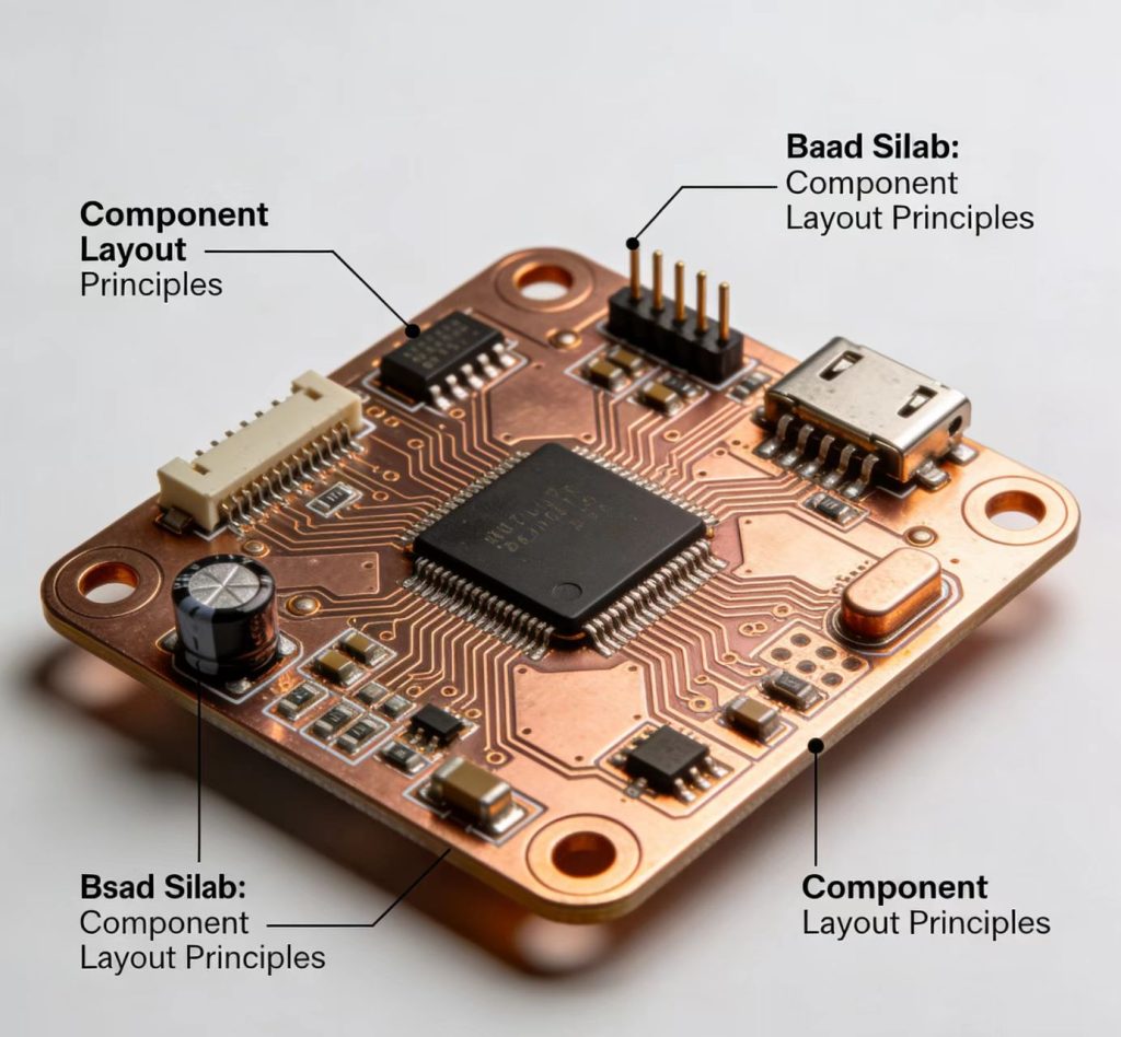
3. Layout and Simulation Optimization
- Component Layout Principles:
3-2-1. Components with power density >0.5 W/cm² should be distributed with spacing ≥2 times of the component height.
3-2-2. Place heat-sensitive components (e.g., crystals) near air inlets, keep a distance of ≥15mm from heat sources.
3-2-3. Design power paths and thermal dissipation paths paralleled, avoiding sharp bends over 90°
In practical applications, a combined method of “material upgrade + structural optimization” is recommended to maximize thermal performance while controlling costs. For example, combining a thermal-electrical separation structure (reducing thermal resistance by ~60%) with a high thermal conductivity insulation layer (another 15% reduction) can lead to a comprehensive thermal resistance improvement exceeding 70%, while the cost increasing is controlled within 50% .
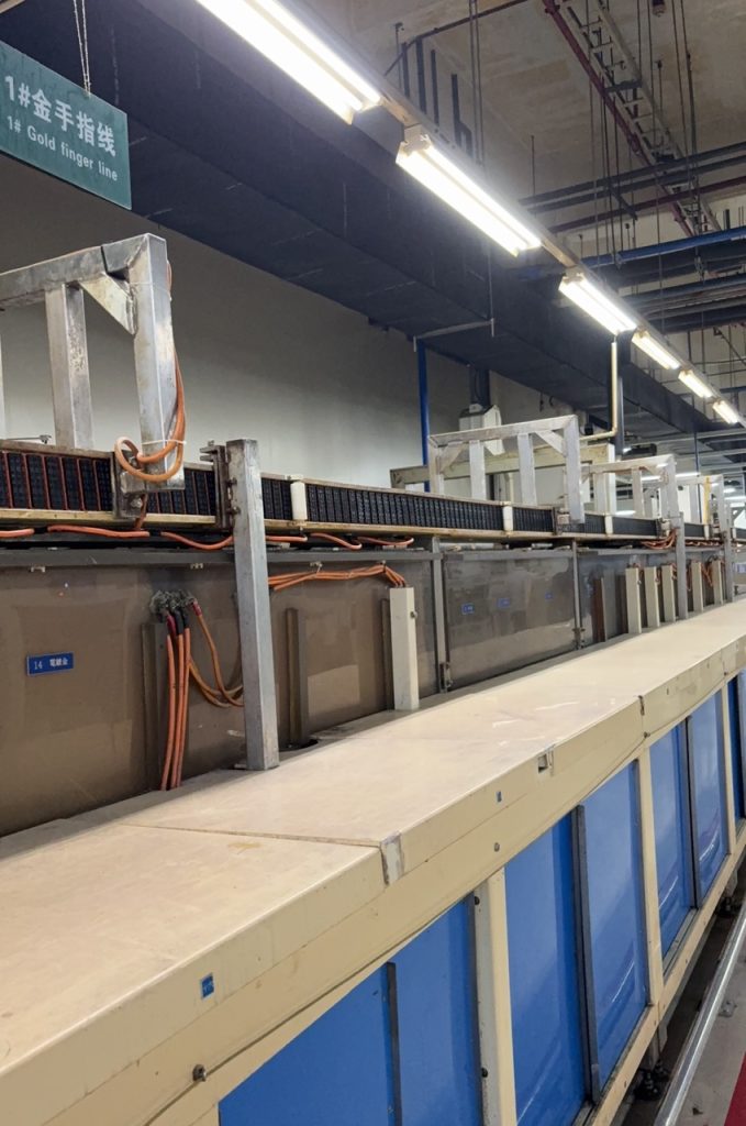
Guangdong Sayfu Multilayer Circuits Co.,Ltd is one of leading enterprise who is focusing on the Copper core PCB technology development, currently we have a capacity of 10000 sq.m per month. Matured technology and quality controlling system with professional management team, your order will be handled without any concerns.