PCB Assembly with advanced SMT Technology- 6 layers Printed circuit board
Images
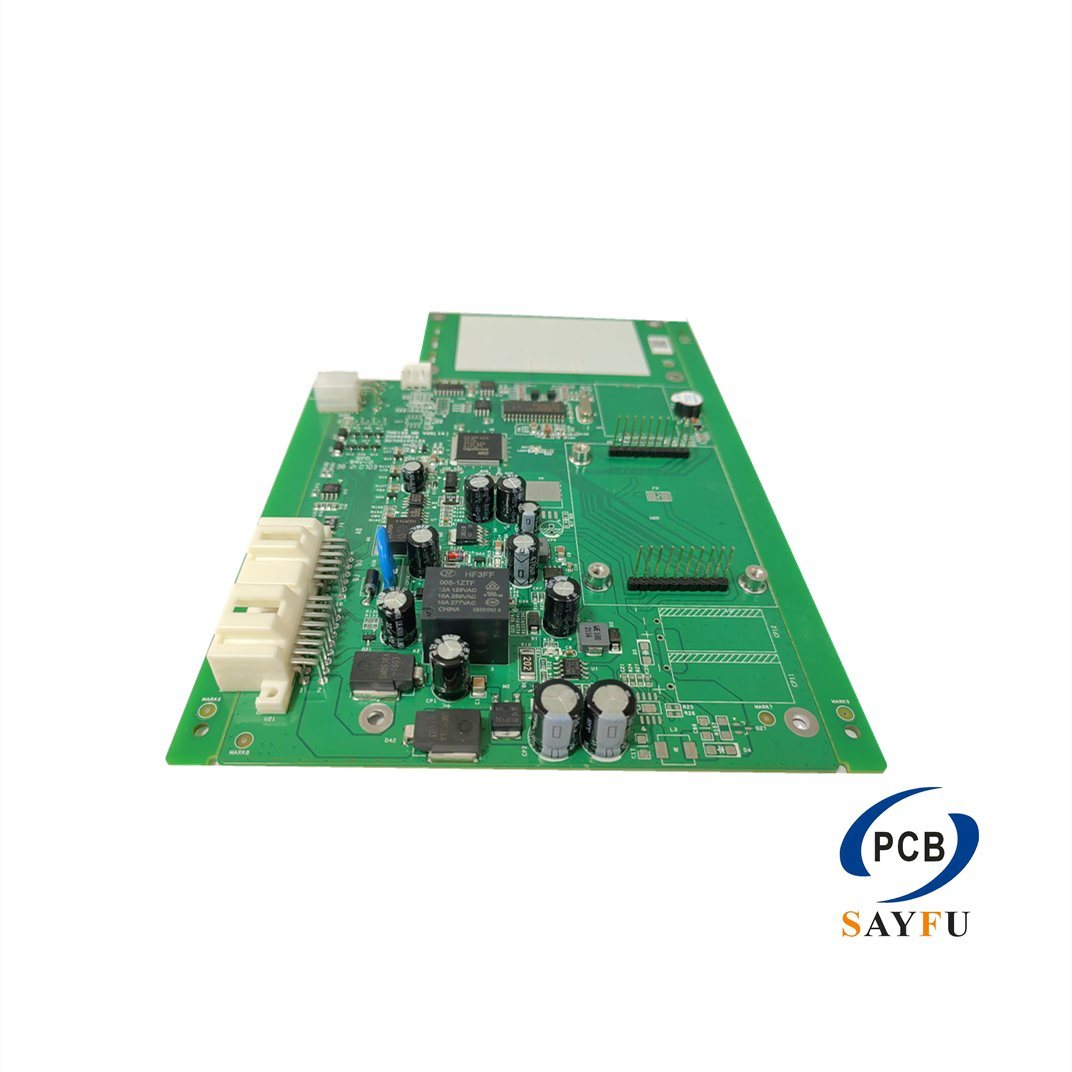
General Specification:
Industrial output main board
IC:0.35mm Pitch(min)
Module:35*35mm
Connector:0.5mm Pitch(min)
Chip:0201(min)
Layer No: 6 layer
Panel size/mm: 175mm*135mm
Material: FR4
Finished Thickess:1.6mm
Finished Copper: 35um
Surface treatment: ENIG
Soldermask: Green
Silkscreen:White
A surface mount technology (SMT Technology) stencil may also be called a PCB sentil, solder paste stencil, or laser stencil.
A SMT Stencil’s main purpose is to simply transfer the solder paste to a bare circuit board.
A stainless steel foil is laser cut to create an opening for each surface mount device on the board.
Once the printed circuit board (PCB) stencil is properly aligned with the top of the board, the solder paste is applied over the openings (in a single pass, with a metal squeegee).
When the stainless steel foil detaches from the board, solder paste remains, ready for the manufacture of the surface-mount device (SMD). In contrast to manual soldering procedures, this process ensures consistency and saves time.
Sayfu provide One stop turnkey partial PCBA. We have 6 sets reflow soldering machine for SMT and 2sets wave soldering machine for DIP. we also have set up small branch for component sourcing which save our customer valuable time and transportation fee.