Turnkey PCB Assembly Solution-2 layers Printed circuit board
Images
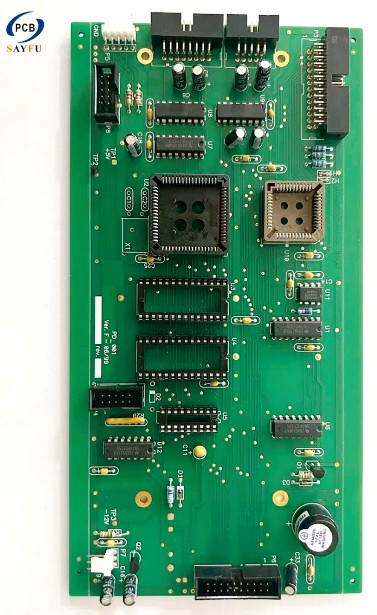
General Specification:
Medical products Main board
IC:0.35mm Pitch(min)
BGA:0.4mm Pitch(min)
connector:0.4mm Pitch(min)
Chip: 0201(min)
Layer No: 4 layer
Panel size/mm: 160mm*125mm
Material: FR4
Finished Thickess:1.6mm
Finished Copper: 35um
Surface treatment: ENIG
Soldermask: Green
Silkscreen:White
SAYFU offer both turn-key and partial turn-key PCB assembly
For full turn-key services, we take care of the entire process, including preparation of Printed Circuit Boards, procurement of electronic components, online order tracking, continuous monitoring of quality and final assembly.
Whereas for partial turn-key, the customer can provide the PCBs and certain components, and the remaining parts will be handled by us.
Printed circuit board assembly (PCB Assembly) and PCB manufacturing are closely linked and are indispensable for the emergence of every new product.
Whether it’s a single pcb, multi-layer, flexible circuit board ,or rigid-flex pcb, our professional team is working to provide one-stop shop for printed circuit board assembly,testing, and commodity sourcing of boards and other materials demands, to provide a comprehensive service from design to delivery, we strive to ensure the most comprehensive manufacturing and testingprocesses to ensure that each board is built and tested to product specifications.
Our company with professional PCB design concept, excellent PCB LAYOUT team, strictdesign process to provide customers with efficient and quality services.
90% of the technical staff have more than 10 years of industry experience, set up a PCB design department, to create more professional services.
To provide PCB package construction for the customer (the customer provides the component DATASHEET).
To provide PCB impedance calculation, lamination design, QA inspection, process inspection, EMC inspection for customers.
The design includes high speed, high frequency, high power, simulation, digital and analog mixing, HDI, soft and hard combination, FPC and other design types.
Master the most advanced technical information, fully consider EMI, EMC and manufacturability design, assist customers and LAYOUT engineers to do schematic diagram analysis and PCB design, to ensure the quality and reliability of the design.
Support schematic diagram and PCB software formats: Cadence, Mentor ee, Mentor pads, Altium (99SE), etc.