High-layer PCB, as the core carriers of electronic devices, are profoundly driving the upgrading of high-end manufacturing industries.
These circuit boards usually have more than 10 layers of conductive layers.
The circuit boards ranging from 10L to 32L are the core components of high-end electronic devices. As the number of layers increases, the integration degree becomes higher;
allowing for the inclusion of more components and meeting the high-density signal transmission requirements of fields such as 5G and AI.
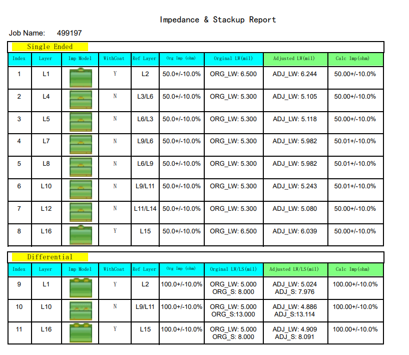
Their manufacturing requires overcoming challenges such as inter-layer alignment and impedance control. The inter-layer error needs to be controlled at the micron level to avoid signal interference.
These circuit boards not only drive the development of equipment towards miniaturization and high performance,but also play a key role in fields such as new energy vehicles and aerospace, and become an important support for technological breakthroughs in the electronic industry.
High-layer PCB – High Precision and High Endurance
They achieve three-dimensional wiring through precise laminating technology,
And can accommodate a large number of components within a limited space, meeting the demands for high-density signal transmission in 5G base stations, autonomous driving chips, aerospace equipment, and other fields.
The manufacturing process will be regard as a perfect example of precision manufacturing.
Employing high-precision impedance control technology to reduce signal loss and interference;
The inter-layer alignment error will be controll within 5 microns to ensure the overall performance is stable.
High-layer PCB these technical challenges make them a crucial indicator for measuring a country’s electronic manufacturing capabilities.
High-layer PCB Green and Low-carbon Manufacturing
Nowadays, as intelligent terminals continue to evolve towards miniaturization , the demand for high multi-layer PCBs is continuously increasing.
It not only enhances the functionality of the equipment, but also providing support for green and low-carbon manufacturing and becoming an important link connecting the digital world and the physical industry.