PCB assembly capabilities for prototypes, NPI builds and volume production — covering SMT, through-hole, BGA assembly, component sourcing, inspection and customer-defined testing.
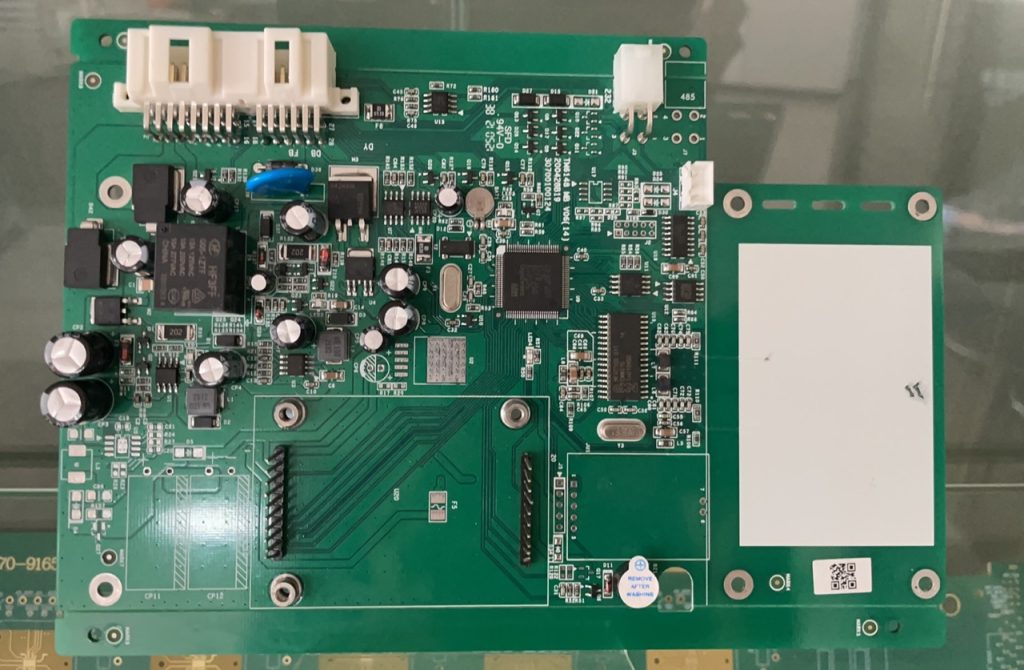
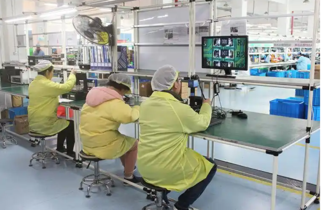
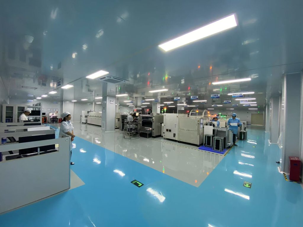
| 15 SMT Lines | ±0.035 mm Placement Accuracy |
| IC Placement ±0.025 mm | 20-Zone Reflow Oven |
| Min. Component: 01005 | Max. PCB: 800 × 600 mm |
PCB Assembly Capabilities at a Glance
SAYFU supports PCBA projects from engineering samples and NPI through to stable volume production. Assembly process, inspection coverage and testing scope are defined based on board complexity, component packages and project requirements — not applied as a fixed standard to every order.
| Capability Area | Detail |
|---|---|
| Assembly Types | SMT, through-hole, mixed-technology (dual reflow + wave) |
| Board Sides | Single-sided and double-sided SMT |
| Min. Component Size | 01005 chip; 0.25 mm pitch |
| Min. BGA Pitch | 0.35 mm |
| Min. QFN Pitch | 0.35 mm |
| Max. IC Package | 45 × 45 mm |
| Max. Connector Size | W45 × L100 mm |
| Max. PCB Size | 800 × 600 × 1.6 mm |
| Max. PCB Layers | 1-30 layers |
| PCB Types | Rigid, multilayer, HDI, flex, rigid-flex, aluminum, high-frequency |
| Production Stages | Prototype, NPI, low-volume, volume production |
| Sourcing Models | Full turnkey, partial turnkey, consigned assembly |
| Process Inspection | 3D SPI, FAI, AOI (140 FPS), X-Ray μCT (Ruby FP), visual inspection |
| Testing Support | ICT, FCT, aging and customer-specific testing |
| Engineering Review | Gerber, BOM, CPL, assembly drawing, special notes |
Projects involving BGA rework, PoP assembly, specialty substrate materials or custom test requirements are evaluated on an individual basis.
→ [SMT Assembly] → [BGA Assembly] → [Testing & Inspection] → [PCB Manufacturing Capability]
Assembly Processes and Component Support
SMT Assembly
SAYFU operates 15 SMT production lines supporting single-sided and double-sided placement, including flex PCB SMT assembly. The line handles components from 01005 passives at 0.25 mm pitch through to large IC packages up to 45 × 45 mm and connectors up to W45 × L100 mm, with a maximum PCB size of 800 × 600 mm.
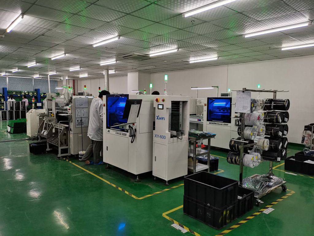
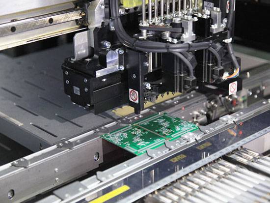
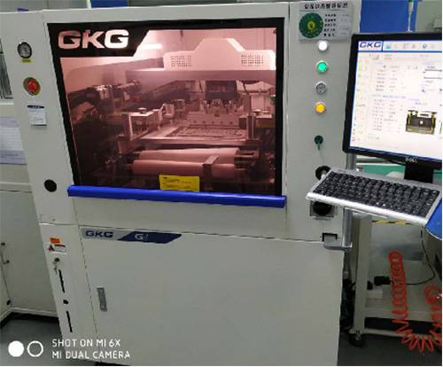
Placement accuracy is ±0.035 mm for standard components and ±0.025 mm for ICs. The reflow oven runs 20 heating zones with ±1°C thermal control, and the line supports through-hole reflow and dual reflow with a single wave pass for mixed-technology boards.
Why these parameters matter for your project:
Placement accuracy of ±0.035 mm is what makes 0.35 mm pitch BGA and QFN placement reliable. At this pitch, the gap between adjacent pads is roughly 0.2 mm — positional error beyond the tolerance directly affects solder joint formation and cannot be corrected after reflow.
Double-sided SMT reflow requires the second pass to be run with components already soldered on the first side. The 20-zone oven allows independent temperature zones across different board regions, managing the thermal mass difference between dense and sparse areas and reducing the risk of component displacement or solder joint re-melt on the underside.
Thermal control at ±1°C is particularly relevant for heat-sensitive components such as crystal oscillators, aluminium electrolytic capacitors and optical devices, and for multilayer boards where different regions absorb heat unevenly.
BGA and Fine-Pitch Assembly
SAYFU supports BGA assembly down to 0.35 mm pitch and QFN assembly down to 0.35 mm pitch, with connector placement down to 0.4 mm pitch. BGA and QFN reliability is determined by four interdependent process stages — not by placement alone.
Assembly process for BGA and fine-pitch devices:
3D SPI → Precision Placement → Controlled Reflow → X-Ray μCT Inspection
Stage-by-stage:
3D SPI — before placement. Paste volume, height and offset are measured at 0–450 μm inspection depth before any component is placed. For BGA at 0.35 mm pitch, incorrect paste volume at this stage cannot be corrected downstream.
Precision placement — ±0.035 mm / IC ±0.025 mm. At 0.35 mm BGA pitch, the solder ball-to-ball gap is approximately 0.2 mm. Placement accuracy at this level is the minimum required for consistent ball alignment across a full BGA array.
Controlled reflow — 20 zones, ±1°C. BGA solder ball wetting, collapse height and joint geometry are determined during reflow. Thermal profile consistency across the board affects ball sphericity and connection strength uniformly across the array.
X-Ray μCT inspection — Ruby FP, resolution <0.1 μm, 160 kV / 10 W. BGA and QFN solder joints are concealed beneath the package body — they cannot be inspected by AOI or visual methods. The Ruby FP supports μCT 3D axis scanning, which produces cross-sectional analysis of individual solder joints rather than flat 2D projection images. This allows detection of internal voids and cracks that a standard 2D X-Ray would miss.
Through-Hole and Mixed Assembly
SAYFU supports through-hole component insertion with wave soldering, through-hole reflow and manual soldering. Mixed SMT and THT boards are handled in a standard dual reflow plus single wave pass sequence. Large connectors, transformers, power components and odd-form parts are supported up to W45 × L100 mm within the 800 × 600 mm maximum board size.
Process selection for mixed boards:
Through-hole reflow allows compatible THT components — typically heat-tolerant connectors and terminal blocks — to be soldered in the same reflow pass as SMT components, eliminating a separate wave pass and reducing handling.
Wave soldering is applied where THT component density is high or where board geometry makes through-hole reflow impractical.
Supported PCB Types
SAYFU provides assembly services for the following PCB types:
- Rigid PCB
- Multilayer PCB
- HDI PCB
- Flex PCB
- Rigid-Flex PCB
- Aluminum PCB
- High-Frequency PCB
Fabrication parameters — including layer count, copper thickness, minimum line and space, impedance tolerance and surface finish options — are covered on the PCB Manufacturing Capability page.
Equipment and Process Capability
| Equipment / Process | Capability Data | Why It Matters for Your Project |
|---|---|---|
| SMT Placement | ±0.035 mm accuracy; IC ±0.025 mm; chip range 01005 to 55 × 55 mm; connector up to W45 × L100 mm | Enables reliable placement of fine-pitch BGA, QFN and high-density ICs without positional defects |
| Stencil Printing | Printing accuracy ±18 μm; supports 01005 and 0.25 mm pitch | Consistent paste volume is the foundation of reliable solder joints — especially for BGA and QFN where paste offset cannot be corrected after reflow |
| 3D SPI | Dual 3D cameras; Moiré lighting; 2D color algorithm; inspection height 0–450 μm | Measures paste volume, height and offset before placement — defects caught at this stage cannot propagate into reflow |
| Reflow Oven | 20 heating zones; ±1°C thermal control | Supports independent zone profiling for multi-layer boards, double-sided reflow and heat-sensitive components |
| AOI | 140 FPS; telecentric lens; 5th-generation coaxial LED lighting | Detects missing, shifted, reversed and tombstoned components across the full board surface after placement |
| FAI (First Article Inspection) | Automated programming; automatic judgement; auto-generated FAI report | Verifies every component value, orientation and polarity before batch production starts — systematic errors found at first article do not reach the batch |
| X-Ray Inspection — Ruby FP | Resolution <0.1 μm; 160 kV / 10 W; μCT 3D axis | Inspects hidden solder joints under BGA, QFN and LGA; μCT 3D cross-section analysis identifies internal voids and cracks not visible in flat 2D imaging |
| Wave Soldering | Dual reflow + single wave pass | High-throughput through-hole soldering for mixed-technology boards |
| Through-Hole Reflow | Integrated into SMT reflow process | Allows compatible THT components to be soldered alongside SMT in the same reflow pass, reducing process steps |
Inspection, Testing and Quality Gates
Process Inspection and Quality Gates
Inspection at SAYFU is structured as a series of quality gates across the production sequence. Each gate targets a different defect type at the point where it can still be corrected or contained.
Inspection sequence:
IQC → 3D SPI → First Article Inspection → AOI → X-Ray (μCT) → Visual Inspection → OQC
| Inspection Method | Equipment | Main Purpose |
|---|---|---|
| IQC (Incoming Quality Control) | — | Verify component identity, package condition and incoming quality before production starts |
| 3D SPI | Dual 3D cameras; Moiré lighting; 0–450 μm inspection depth | Measure solder paste volume, height and offset before any component is placed |
| FAI (First Article Inspection) | Automated programming; auto-generated report | Verify every component value, orientation and polarity on the first assembled board before batch build begins |
| AOI | 140 FPS; telecentric lens; coaxial LED | Detect missing, shifted, reversed and tombstoned components after placement and reflow |
| X-Ray — Ruby FP | Resolution <0.1 μm; 160 kV / 10 W; μCT 3D axis | Inspect hidden solder joints under BGA, QFN and LGA packages |
| Visual Inspection | — | Check connectors, mechanical assembly, workmanship and any board areas outside automated coverage |
| OQC (Outgoing Quality Control) | — | Confirm inspection and test records are complete before shipment is released |
Electrical and Functional Testing
Testing scope is defined per project. The methods below are available; which apply depends on board complexity, customer-provided materials and the agreed test specification.
| Test Type | Main Purpose | What the Customer Needs to Provide |
|---|---|---|
| ICT (In-Circuit Test) | Check shorts, opens, component values and network continuity | Test point definitions and fixture requirements |
| FCT (Functional Circuit Test) | Verify product functions against defined acceptance criteria | Test procedure, firmware and pass/fail criteria |
| Power-On Test | Confirm basic startup and power-rail behaviour | Power conditions and pass/fail criteria |
| Aging Test | Verify operation under defined duration and load conditions | Duration, load profile and environmental conditions |
| Firmware Programming | Program MCU, FPGA or other programmable devices | Firmware file and programming instructions |
| Custom Test | Project-specific verification | Test specification and reference sample |
Send Your PCB Assembly Files for Engineering Review
Submit your Gerber files, BOM, Pick-and-Place data and assembly drawing. SAYFU’s engineering team will review assembly compatibility, component risks, inspection coverage and testing requirements before production starts.