Fine-Pitch SMT Assembly for 6-Layer Industrial Control Boards
Images
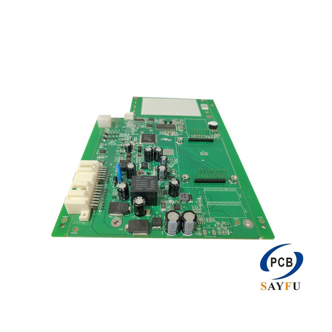
General Specification:
Industrial output main board
IC:0.35mm Pitch(min)
Module:35*35mm
Connector:0.5mm Pitch(min)
Chip:0201(min)
Layer No: 6 layer
Panel size/mm: 175mm*135mm
Material: FR4
Finished Thickess:1.6mm
Finished Copper: 35um
Surface treatment: ENIG
Soldermask: Green
Silkscreen:White
This 6-layer PCB assembly targets industrial output main boards that combine fine-pitch ICs, small passives, and connectors on a single panel. The assembly process supports IC pitches down to 0.35 mm, connector pitches down to 0.5 mm, and passive components as small as 0201 — a combination suited to compact control boards where component density is high.
SAYFU builds this board with FR-4 material, 1.6 mm finished thickness, 35 μm finished copper, and ENIG surface finish. Fabrication and assembly support covers prototypes, low-volume runs, and repeat production from customer-supplied design files.
If your layout requires IC pitch below 0.35 mm or connector pitch below 0.5 mm, send your BOM and footprint so we can confirm feasibility before you finalize the design — this spec reflects our standard fine-pitch line, not the absolute limit of every process on the floor.
Why Fine-Pitch Assembly Matters Here
Placing 0.35 mm-pitch ICs and 0201 passives on the same 175 × 135 mm panel leaves little margin for solder paste, placement, or reflow error. Solder paste printing, stencil opening design, and reflow profile all get reviewed before production specifically to catch issues that fine-pitch layouts are prone to: solder bridging between tight pads, insufficient solder on small terminations, and placement shift during reflow.
Component orientation and pad spacing get checked against the pick-and-place data before the first run, not after — catching a footprint mismatch at review is far cheaper than reworking a populated panel.
PCB Construction and Surface Finish
The 6-layer FR-4 stack-up gives control circuits, power distribution, communication interfaces, and ground planes separate routing layers, which matters once connector count and trace density go up on an I/O-heavy board like this one.
ENIG’s flat pad surface holds up for both fine-pitch component soldering and connector plating on the same board — that combination is why it’s the standard finish here rather than HASL, which doesn’t stay flat enough at 0.35 mm pitch.
Stack-up, copper weight, impedance requirements, material grade, and surface finish can all shift based on your design and operating environment; the specs below are the standard configuration for this board type.
Technical Specifications
| Item | Specification |
|---|---|
| Product Type | Industrial Control PCB Assembly |
| PCB Layer Count | 6 Layers |
| PCB Material | FR-4 |
| PCB Size | 175 × 135 mm |
| Module Size | 35 × 35 mm |
| Finished Thickness | 1.6 mm |
| Finished Copper Thickness | 35 μm |
| Surface Finish | ENIG |
| Minimum IC Pitch | 0.35 mm |
| Minimum Connector Pitch | 0.5 mm |
| Minimum Component Size | 0201 |
| Solder Mask | Green |
| Silkscreen | White |
Assembly Inspection and Quality Control
Gerber files, BOM, pick-and-place data, polarity marks, and assembly drawings get reviewed for manufacturability before assembly starts. Given the fine-pitch components on this board, that review focuses on footprint and stencil accuracy in particular — the two things most likely to cause defects at 0.35 mm pitch.
Depending on your component layout and requirements, the inspection plan may include:
- Solder paste inspection
- First-article inspection
- Automated optical inspection
- X-ray inspection for hidden solder joints (e.g., under fine-pitch QFN packages)
- Visual inspection
- Electrical or functional testing per your test procedure
Confirm the inspection and testing plan with us before production so the coverage matches your board’s risk points, not a generic checklist.
Industrial Applications
This assembly fits boards where fine-pitch ICs, connectors, and mixed through-hole/SMT components sit on the same panel — common in:
- Industrial control systems and PLCs
- Factory automation equipment
- Motor and power control units, where connector density is high
- Human-machine interfaces, where small-pitch connectors and mixed mounting are typical
- Monitoring and measurement devices
- Embedded control modules
Material, component, and reliability requirements still depend on your operating temperature, vibration, electrical load, and expected product life — the applications above indicate fit, not a guarantee of suitability without design review.
Custom Industrial PCB Assembly
If your design uses fine-pitch ICs (≤0.35 mm), small connectors (≤0.5 mm), or 0201 passives on a multilayer board, this line’s capability fits your requirements. For designs outside that range, send your files for a manufacturability review before quoting.
SAYFU customizes layer count, board dimensions, material, copper thickness, surface finish, component packages, testing scope, and production quantity based on your design.
For a quotation and manufacturability review, provide:
- Gerber files
- Bill of Materials
- Pick-and-place file
- Assembly drawing
- Testing requirements
- Expected production quantity
Send your project files to get a PCB assembly quotation and engineering review.