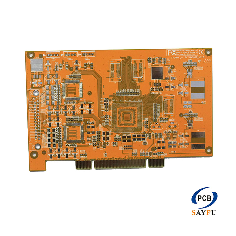
Differences Between PTH PCB and HDI PCB
PTH PCB is the main product of Printed Circuit Boards (PCBs), which are essential in electronics, along with High-Density Interconnect (HDI) PCBs representing distinct technologies catering to different needs.
Technology and Structure:
PTH PCB rely on mechanically drilled through-holes (typically >0.2 mm in diameter) coated with copper to connect layers. Components are mounted by inserting leads into these holes and soldering them, providing strong mechanical bonds but limiting density.
-HDI PCBs use laser-drilled microvias (<0.1 mm diameter), blind vias (connecting outer to inner layers), and buried vias (internal layer connections). This allows for finer traces (as narrow as 50 μm) and higher component density.
Performance and Applications of PTH PCB and HDI PCB:
PTH PCB is suitable for low-frequency, less complex applications (e.g., power adapters, basic consumer electronics) due to their robustness but suffer from longer signal paths, leading to signal loss and interference in high-frequency scenarios.
HDI PCBs enable shorter signal paths, reducing delay and attenuation by over 60%. This improves signal integrity, making them ideal for high-speed, high-frequency applications like smartphones, 5G equipment, and medical devices.
Manufacturing and Cost :
PTH PCB involves simpler processes like mechanical drilling and electrolytic copper plating, resulting in lower costs for low-density designs.
HDI PCBs require advanced techniques like sequential lamination, laser drilling, and electroless copper plating, increasing initial costs but offering better miniaturization and performance.
Design Flexibility :
Rigid PCB face limitations in layer stacking and space utilization, as through-holes occupy significant area.
HDI PCBs support arbitrary layer interconnections (any-layer HDI), allowing complex routing in compact form factors.
In summary, while PTH PCBs prioritize mechanical strength and cost-effectiveness for simpler applications, HDI PCBs excel in miniaturization, high-speed performance, and complexity, driving innovation in modern electronics.
Sayfu Group can manage not only normal multilayer circuits but also HDI boards, if you have met problems, just come to us for any quesitons. With 20 more years development, although now in China the total capacity is high more than the actual demand of world wild, we are fighting to grow stronger on quality and service.