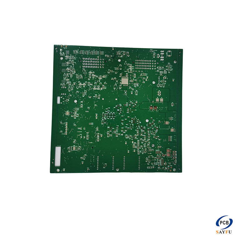
PC boards design is an important phase of PCB/PCBA products. While vias are an important knowledge point. Especially for high-speed multilayer PC boards design, the design of vias needs to attract the attention of engineers.
Let’s understand the knowledge of vias in PC boards design.
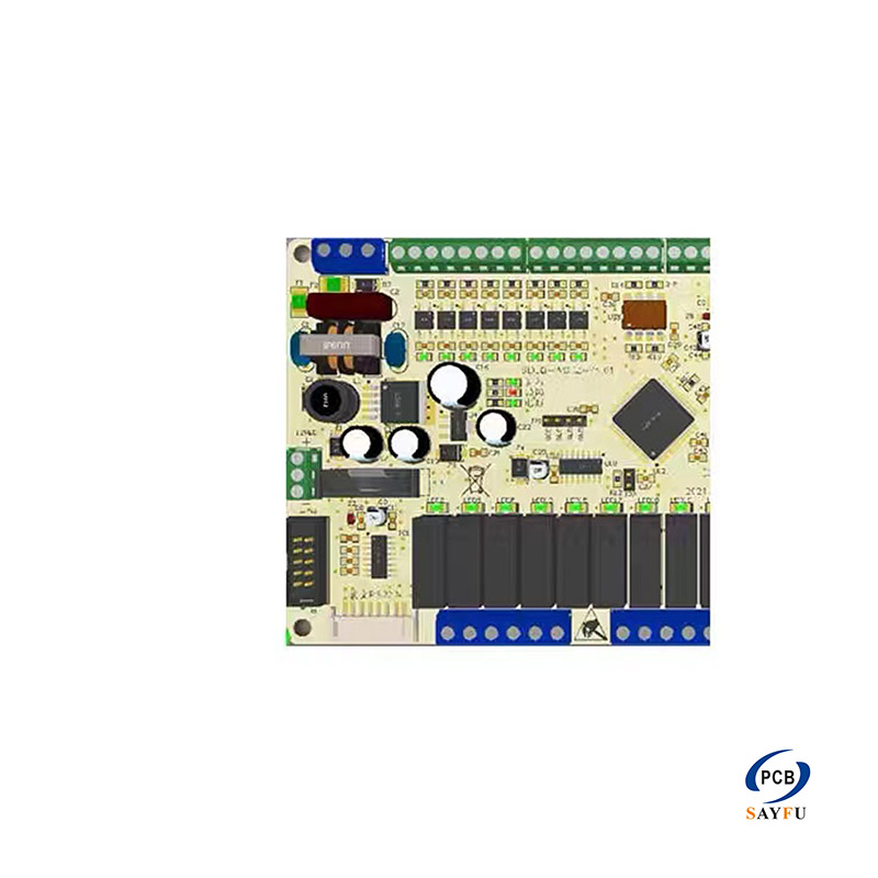
Vias are generally divided into three categories: through holes, blind holes, and buried holes.
Blind hole: refers to the surface of the top and bottom layers of the printed circuit board, which has a certain depth and is used for the connection between the surface layer circuit and the inner layer circuit below. The depth of the hole and the aperture usually do not exceed a certain ratio.
Buried hole: refers to the connection hole located in the inner layer of the printed circuit board, it will not extend to the surface of the circuit board.
Through hole: This kind of hole penetrates the whole circuit board, and can be used for internal interconnection or as a positioning hole for component installation. Because the through hole is easier to realize in the process and the cost is lower, it is generally used in printed circuit boards.