PCB proofing
Circuit board electronic component, also known as printed circuit board, printed circuit board is an important electronic component is the support body of electronic components is the provider of electrical connection of electronic components. Because it is made by electronic printing, it is called “printed” circuit board.
PCB proofing refers to the trial production of printed circuit boards before mass production. Mainly used for electronic engineers in the design of a good circuit and complete the PCB Layout to the factory after the small batch trial production process is PCB proofing. The production quantity of PCB proofing generally has no specific boundary line. Generally, engineers call it PCB proofing before confirming and testing the product design.
Circuit board welding process
1.PCB board welding process
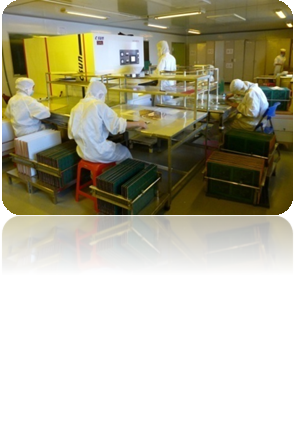
- 1.1 Introduction to PCB board welding process. PCB board welding process requires manual plug-in, manual welding, repair and inspection.
- 1.2 PCB board welding process. List components – plugins – welding – clippers – inspection – trimming

Printed circuit board welding process requirements
2.1 Process requirements for components processing
- 2.1.1 Before the components are installed, the weldability of the components must be treated. If the weldability is poor, tin plating shall be performed on the pins of the components.
- 2.1.2 After shaping the pin of the component, the pin spacing shall be consistent with the pad hole spacing of the PCB board.
- 2.1.3 The processed shape of the pin of the component shall be conducive to heat dissipation during the component welding and mechanical strength after welding.
2.2 Process requirements for components to be inserted on Printed circuit board
- 2.2.1 Components shall be installed in the order of low before high, small before large, light before heavy, easy before difficult, general components before special components, and the installation of the previous procedure shall not affect the installation of the next procedure.
- 2.2.2 After the component is installed, the logo shall be read in a direction that is easy to read and from left to right as far as possible.
- 2.2.3 Polarity of polar components shall be installed in strict accordance with the requirements on the drawings and shall not be misinstalled.
- 2.2.4 The components shall be evenly distributed and neatly arranged on the PCB board. Oblique, three-dimensional cross and overlapping arrangement are not allowed. One side is not allowed to be high while the other side is low; It is also not allowed for pins to be long on one side and short on the other.
2.3 PCB board welding joint process requirements
- 2.3.1 The mechanical strength of solder joints shall be sufficient.
- 2.3.2 Welding is reliable and conductive performance is guaranteed.
- 2.3.3 The surface of solder joints shall be smooth and clean
Electrostatic protection during printed circuit board welding
3.1 PRINCIPLES of ESD Prevention
- 3.1.1 Prevent the accumulation of static electricity in places where static electricity may be generated, and take measures to control it within the safety range.
- 3.1.2 The existing static electricity accumulation should be eliminated quickly and released immediately.
3.2 ESD Prevention Methods
- 3.2.1 Leakage and grounding. Ground the parts that may or have generated static electricity to provide an electrostatic discharge channel. The method of burying ground wire is used to establish “independent” ground wire. Elimination of non-conductor with static electricity: use ion fan to produce positive and negative ions, and static power static electricity
Importance of PCB electronic component proofing
In the proofing process is likely to find a variety of problems on the board, so as to improve. This is to carefully choose the number of proofing, in order to effectively control the cost. So the number of 5, 10 tablets is very common. Secondly, the PCB board designed by different engineers is not the same information, the size of the board is not the same, 5cm5cm, 10cm10cm and other sizes have! However, the size of raw materials for PCB processing is generally 1.21m. If a 1.2x1m raw material board is only used to produce five PCB boards of 10cm10cm, the waste of this material will be obvious, and the increase of cost is what both the supply and demand do not want to see.
Therefore, PCB Prototype proofing manufacturers in order to save costs and improve production efficiency, different customers, different sizes, the same process of PCB board together for processing and production, and then cut the shipment to customers.
Splicing has an advantage, if the cost is not considered, splicing is still beneficial, not to mention the quantity, after confirming the sample, the following production, there will be a lot of problems. The ability to CUT through the foot, the ability to close the v-cut between the boards, these are all important information. So there’s still a place for jigsaw.