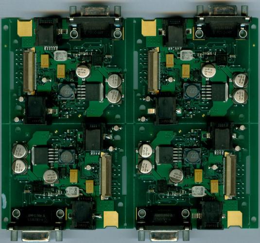
High Density Interconnect PCB
High Density Interconnect PCB, is a well-known concept you need to know about. It is an important so you need to learn about(HDI PCB) and its benefits ASAP.
Key HDI advantages
The evolution of excessive-density pcb generation has given engineers more design freedom and flexibility than ever before. Designers use HDI methods now can put more components on both sides of the PCB if they want. In essence, HDI PCB gives the designers more place to design, and put smaller components even more closer together. This means that a HDI PCB could get a more faster signal transmission together with great signal quality.
We use HDI widely to reduce the weight and dimensions of the products, and to improve the electrical performance of the device.The HDI pcbs are widely usded in mobile phones, touch-screen products, computer systems, virtual cameras and communications products.
High Density Interconnector PCB application
High Density Interconnector PCB are appropriate for widely ranges. As above, you will find them in mobile phones, touch-screen products, computer systems, virtual cameras and communications products., they could also be used in all kinds of other digital products, like smartphones, where miniaturization is fundamental to the powerful software of the product. You may also find them in automobiles, planes and different motors that rely upon electronics.
One of the maximum essential field where the High Density Interconnector PCB used is medical field. Medical devices often need small packages with high transmission rates that only High Density Interconnector PCB can supply. For example, an implant needs to be small enough to fit with the human body, however, any electronics involved in must allow for high-speed signal transmission</span&amp;amp;gt;. Therefore, the High Density Interconnector PCB certainly is a godsend. High Density Interconnector PCB can also be beneficial in other medical divices, such as emergency room monitors, CT scans and so on.
No matter you are in what kind of field, you’re probably already getting some ideas about how HDI PCBs can make your electronics products even better. Get touch with us—GuangDong Sayfu, and we discuss it.