With the development of electronic information technology, more and more fields use multi-layer PCB boards.
Traditionally, we define PCB boards with more than 4 layers as “multilayer PCB boards“, and more than 10 layers as “high multi-layer PCB boards“. Whether it can produce high-level multi-layer PCB boards is an important indicator to measure the strength of a PCB board manufacturer. It can produce high-level multi-layer boards with more than 20 layers, which is regarded as a PCB company with top-notch technical strength.
Therefore, the production of multi-layer PCB boards is expensive due to the difficulty. But there will still be people who are very puzzled, where is the difficulty? Is it the difficulty of deliberately increasing the price and making it up? Today, let me explain to you in detail: why is it so difficult to make multi-layer PCB boards?
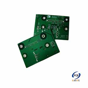
Main production difficulties
Compared with conventional circuit boards, high-level circuit boards have thicker components, more layers, denser lines and vias, larger unit size, thinner dielectric layers, etc., internal space, interlayer alignment, impedance control and reliability. Sexual requirements are more stringent.
- Difficulty in alignment between layers
Due to the large number of layers in the high-rise board, the customer design side has more and more stringent requirements on the alignment of each layer of the PCB. Usually, the alignment tolerance between layers is controlled to ±75μm. Factors such as dislocation stacking and interlayer positioning methods caused by the inconsistency of the expansion and contraction of different core board layers make it more difficult to control the interlayer alignment of high-rise boards. - Difficulties in making inner layers
The high-rise board adopts special materials such as high TG, high speed, high frequency, thick copper, and thin dielectric layer, which puts forward high requirements for inner layer circuit production and graphic size control. The line width and line spacing are small, the open and short circuits increase, the micro-shorts increase, and the pass rate is low; there are many signal layers of fine lines, and the probability of missed inspection of the inner layer AOI increases; the thickness of the inner core board is thin, which is easy to wrinkle, resulting in poor exposure and etching. It is easy to roll the board when the machine is over; the cost of scrapping the finished product is relatively high. - Difficulties in pressing
Multiple inner core boards and prepregs are superimposed, and defects such as sliding plates, delamination, resin voids and bubble residues are prone to occur during lamination production. When designing the laminated structure, it is necessary to fully consider the heat resistance, withstand voltage, amount of glue filling and dielectric thickness of the material, and set a reasonable high-level board pressing program. - Difficulties in drilling production The use of high-TG, high-speed, high-frequency, and thick copper special plates increases the difficulty of drilling roughness, drilling burrs and decontamination. The number of layers is large, the cumulative total copper thickness and plate thickness, and the drilling tool is easy to break; there are many dense BGAs, and the CAF failure problem caused by the narrow hole wall spacing; the inclined drilling problem is easily caused by the plate thickness.
Control of key production processes
- Material selection
Electronic circuit materials are required to have relatively low dielectric constant and dielectric loss, as well as low CTE, low water absorption and better high-performance copper clad laminate materials to meet the processing and reliability requirements of high-level boards. - Laminated structure design
The main factors considered in the design of the laminated structure are the heat resistance of the material, the withstand voltage, the amount of glue filling and the thickness of the dielectric layer, etc. The following main principles should be followed:
(1) Prepreg and core board manufacturers must be consistent. In order to ensure the reliability of PCB, all layers of prepreg should avoid using single 1080 or 106 prepreg (except customers have special requirements). If the customer has no dielectric thickness requirements, the thickness of the dielectric between each layer must be guaranteed according to IPC-A-600G ≥ 0.09mm.
(2) When the customer requires high TG sheet, the core board and the prepreg must use the corresponding high TG material.
(3) If the inner layer substrate is 3OZ or above, use prepreg with high resin content, but try to avoid the structural design of using 106 high resin prepreg.
(4) If the customer has no special requirements, the thickness tolerance of the interlayer dielectric layer is generally controlled by +/-10%. For the impedance plate, the dielectric thickness tolerance is controlled by the IPC-4101 C/M class tolerance. If the impedance influencing factor is related to the thickness of the substrate If relevant, the sheet tolerances must also be in accordance with IPC-4101 Class C/M tolerances. - Interlayer alignment control The accuracy of the size compensation of the inner layer core board and the control of the production size need to be accurately compensated for the graphic size of each layer of the high-rise board through the data collected in production and the experience of historical data for a certain period of time, so as to ensure the expansion and contraction of the core board of each layer. consistency.
- Inner layer circuit technology Since the resolution capability of the traditional exposure machine is about 50μm, for the production of high-level boards, a laser direct imaging machine (LDI) can be introduced to improve the image resolution capability, and the resolution capability can reach about 20μm. The alignment accuracy of the traditional exposure machine is ±25μm, and the interlayer alignment accuracy is greater than 50μm; using a high-precision alignment exposure machine, the pattern alignment accuracy can be increased to about 15μm, and the interlayer alignment accuracy is controlled within 30μm.
- Pressing process At present, the interlayer positioning methods before lamination mainly include: four-slot positioning (Pin LAM), hot melt, rivet, hot melt and rivet combination. Different product structures adopt different positioning methods. For high-rise boards, the four-slot positioning method is used, or the fusion + riveting method is used. The OPE punching machine punches out the positioning holes, and the punching accuracy is controlled at ±25μm.
According to the laminated structure of the high-rise board and the materials used, study the appropriate lamination procedure, set the best heating rate and curve, appropriately reduce the heating rate of the lamination sheet, prolong the high temperature curing time, make the resin flow and cure fully, and avoid pressing Problems such as sliding plate and interlayer dislocation during the combination process.
- Drilling process
Due to the superposition of each layer, the plate and copper layer are super thick, which will seriously wear the drill bit and easily break the drill blade. The number of holes, drop speed and rotation speed should be adjusted appropriately. Accurately measure the expansion and contraction of the board and provide accurate coefficients; the number of layers is greater than or equal to 14 layers, the hole diameter is less than or equal to 0.2mm, or the hole-to-line distance is less than or equal to 0.175mm. Step-by-step drilling, with a thickness-to-diameter ratio of 12:1, is produced by step-by-step drilling, positive and negative drilling methods; control the drilling tip and hole thickness, and use a new drill or a grinding drill for high-rise boards as much as possible, and the hole thickness is controlled within 25um.
Reliability test
High-rise boards are thicker, heavier, and have larger unit sizes than conventional multi-layer boards, and the corresponding heat capacity is also larger. During welding, more heat is required and the welding high temperature time experienced is longer. It takes 50 seconds to 90 seconds at 217°C (the melting point of tin-silver-copper solder), and the cooling rate of the high-level board is relatively slow, so the time for the reflow test is prolonged.