12-Layer HDI PCB with Copper-Filled Vias for Medical Applications
Images
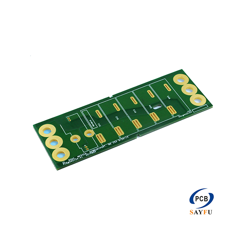
General Specification:
12Layer HDI PCB
Layer counts: 12 Special process
Fill the hole by plated copper
Surface treatment: ENIG
1+1+8+1+1 IPC Class 3
Application: Medical
This 12-layer HDI PCB uses a 1+1+8+1+1 build-up, plated-copper-filled vias, ENIG surface finish, and IPC Class 3 requirements for medical applications. The structure combines an eight-layer core with HDI build-up layers on both sides, creating routing space for a dense medical electronics layout.
Copper-filled vias are part of the special process specified for this product. Their locations, layer spans, and relationship to the component layout need to be shown in the stack-up and drill documentation. The board should be quoted from the completed HDI design package, not from a generic 12-layer description.
Product Overview
The 1+1+8+1+1 structure defines the layer sequence for this board. Include the final stack-up, via map, and any controlled-net requirement with the Gerber files. These items establish how the outer HDI layers connect into the core and which routing areas drive the build-up.
IPC Class 3 is stated for this product. Include the application-specific inspection and documentation requirements with the RFQ so the requested standard is applied to the final board package rather than treated as a general label.
Copper-Filled Via Design
Copper-filled vias can be used where the HDI layout needs a defined via structure beneath or near dense component areas. The exact via positions, drill information, and pad design must come from the final data. Provide the component drawing and placement information where the via structure is tied to a constrained footprint.
ENIG is specified for the exposed pads. Pad geometry and solder mask clearance should match the selected components and the planned assembly method. For a board supplied with components or connectors, send the BOM, placement data, and assembly drawing; related support is described on the turnkey PCB assembly page.
Medical Application Information
This board is identified for medical applications. Include the final application, operating constraints, required documentation, quantity, and inspection expectation with the quotation files. The PCB manufacturing capabilities page provides related context for HDI and multilayer projects.
What to Confirm Before Production
Please provide Gerber files, drill files, the 1+1+8+1+1 stack-up, and the copper-filled-via map. Include the ENIG requirement, IPC Class 3 requirement, component or connector drawings where applicable, and the requested inspection information. This gives the quote a defined basis for reviewing the HDI structure and medical application requirements.