CSP IC Substrate for Compact Chip-Scale Package Applications
Images
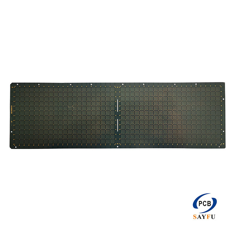
General Specification:
Number of layers: 2/4 floors mainly
Structural features: thinner substrate core, more blind and buried via structures
Size: 44mm~1919mm
Board thickness: 0.1~0.4mm
Line width/line distance: 25/25 ~ 50/50 um
Gold finger spacing: 75~130 um
Surface treatment: Soft Au \ AFOP \ OSP
Special process: TLP, Etch back, VIP, VOP
CSP IC substrate is used for chip-scale package applications where the package size is close to the size of the IC itself. This product mainly supports 2/4-layer CSP substrate structures, thin substrate cores, more blind and buried via structures, 0.1-0.4 mm board thickness, 25/25-50/50 um line width and spacing, 75-130 um gold finger spacing, Soft Au / AFOP / OSP surface treatment, and TLP, etch back, VIP, and VOP special processes.
The original product detail identifies CSP as a single-chip package type used in memory products, telecommunication products, RF devices, and electronic products with a small number of pins. For buyers, the important value is the combination of thin substrate design, fine routing, dense via structures, and package-level surface treatment options.
Why CSP Substrate Parameters Matter
CSP packaging reduces the distance between the chip and the board-level interconnect compared with larger package forms. Shorter signal paths can support compact layouts and help improve electrical behavior when the package structure is suitable for the application.
The 0.1-0.4 mm board thickness and thin substrate core make this product suitable for light, thin, and small electronic products. At this size range, substrate flatness, via structure, line spacing, and surface treatment all become important for package assembly and reliability.
Fine Routing, Via Structure, and Gold Finger Spacing
The 25/25-50/50 um line width and spacing supports compact routing in chip-scale package substrates. This routing range should be reviewed together with the package layout, chip function, solder ball or contact structure, and inspection requirements.
The product also uses more blind and buried via structures, which help route signals in a compact substrate without consuming unnecessary surface area. The 75-130 um gold finger spacing should be confirmed when the package design includes contact areas that require tight spacing control.
Surface Treatment and Special Processes
The available surface treatment options include Soft Au, AFOP, and OSP. The right finish should be selected according to the package connection method, contact requirement, assembly process, and storage condition.
The special process options include TLP, etch back, VIP, and VOP. These should be clearly defined in the substrate design package because they can affect via formation, surface quality, package assembly, and reliability.
For related process background, see IC substrate PCB capabilities and the IC substrates product category.
Quality Control and Manufacturing Review
For CSP IC substrates, manufacturing review should focus on thin-core handling, blind and buried via reliability, fine-line registration, gold finger spacing control, surface finish selection, and special process consistency. These factors directly affect whether the substrate can support a compact chip-scale package.
Because the chip particles are connected through solder balls or package-level contacts, the PCB-side contact area and substrate structure must support electrical connection, mechanical support, and heat transfer in a compact form.
Typical Applications
CSP IC substrate is suitable for compact electronics where chip-scale packaging helps reduce product size and support lightweight design. Typical applications include:
- Memory products
- Telecommunication products
- RF devices
- Microprocessor or controller applications
- ASIC-related products
- Mobile electronic devices such as smartphones and digital cameras
The final fit depends on package design, chip function, routing density, thermal requirement, and reliability target.
Custom CSP IC Substrate Manufacturing
SAYFU can manufacture CSP IC substrates based on customer-supplied package drawings, substrate design files, connection requirements, surface treatment requirements, and production quantity. For this product type, the 2/4-layer structure, 0.1-0.4 mm thickness, 25/25-50/50 um routing, 75-130 um spacing, Soft Au / AFOP / OSP finish, and TLP / etch back / VIP / VOP process requirements should be reviewed together.
For quotation and manufacturability review, provide:
- Package drawings
- Substrate design files
- Gerber data if available
- Blind and buried via requirements
- Gold finger or contact spacing requirements
- Surface treatment selection
- TLP, etch back, VIP, or VOP process notes
- Target application and reliability requirements
- Expected production quantity
For broader design preparation questions, see the FAQ on design and technical issues.