Flip Chip CSP PCB Board for Low-Loss IC Substrate Applications
Images
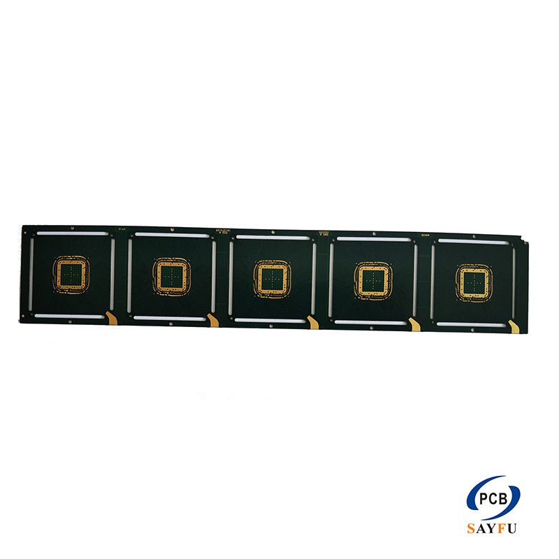
General Specification:
Number of layers: 2/4 layers
Structural features: There are many blind hole filling structures. The electrical connection design of the chip area includes SOP (Sold On Pad) or BOL (Bump On Line) design.
Size: 88mm~1214mm
Board thickness: 0.2~0.4mm
Line width/line distance: 25/25~50/50 um
Bump Pitch: 150~200um
Surface treatment: OSP
Special process: VOP
Flip Chip CSP PCB board is used for package structures where the chip is flipped to create a compact, direct connection path. This product supports 2/4-layer IC substrate designs, blind hole filling structures, SOP (Sold On Pad) or BOL (Bump On Line) chip-area connection designs, 0.2-0.4 mm board thickness, 25/25-50/50 um line width and spacing, 150-200 um bump pitch, OSP surface treatment, and VOP special process.
The product belongs to the IC substrate and advanced package board family rather than a standard rigid PCB use case. It is suitable when the package must support compact electronic products, processors, communication hardware, or other applications where signal path length, bump pitch, and thermal behavior matter.
Why Flip Chip CSP Structure Matters
In a flip chip package, the chip connection can shorten the signal path and reduce losses compared with less direct interconnect structures. This makes FC-CSP useful for designs where package density, electrical behavior, and heat transfer must be handled in a compact space.
The 2/4-layer structure and 0.2-0.4 mm substrate thickness support thin package construction. At the same time, 150-200 um bump pitch and fine line spacing require careful routing, pad design, and process control before fabrication.
Chip-Area Connection and Fine Routing
The chip area can use SOP or BOL electrical connection design depending on the package layout. These connection structures need to match the chip package layout, bump arrangement, and substrate routing strategy.
The 25/25-50/50 um line width and spacing range is suitable for dense package routing, but it also means CAM review, layer registration, and inspection planning are important. Blind hole filling structures can help support compact interconnects and cleaner surface preparation for later assembly.
Surface Treatment and VOP Process
OSP surface treatment provides a solderable organic finish for the package substrate. For flip chip CSP applications, the surface finish should be considered together with bump pitch, chip-area pad design, and assembly timing.
The VOP special process should be clearly specified in the design package. For this product, VOP, blind hole filling, bump pitch, and SOP/BOL design should be reviewed as one process group rather than separate line items.
For related capability context, see IC substrate PCB capabilities and the IC substrates product category.
Quality Control and Manufacturing Review
For Flip Chip CSP PCB boards, production review should focus on bump pitch control, fine-line registration, blind hole filling, SOP/BOL pad structure, OSP surface condition, and VOP process consistency. These details affect signal connection, assembly reliability, and thermal behavior.
Package drawings, substrate design files, chip package information, signal requirements, thermal notes, and reliability expectations help the manufacturing team confirm whether the board should be handled through IC substrate capability.
Typical Applications
Flip Chip CSP PCB boards are relevant for compact and advanced electronic products where package size, signal behavior, and thermal performance are important. Typical application directions include:
- Smartphone processors
- PC microprocessors or controllers
- Video processors
- Audio processors
- Compact communication and network electronics
- Advanced package designs that need short signal paths and controlled bump pitch
IC substrate boards can also support lightweight and thin electronic products when the design requirements support this package approach.
Custom Flip Chip CSP PCB Manufacturing
SAYFU can manufacture Flip Chip CSP PCB boards based on customer-supplied package drawings, substrate files, chip-area connection requirements, surface treatment requirements, and production quantity. For this product type, the 2/4-layer structure, 0.2-0.4 mm thickness, 25/25-50/50 um routing, 150-200 um bump pitch, OSP finish, blind hole filling, and VOP process should be reviewed together.
For quotation and manufacturability review, provide:
- Package drawings
- Substrate design files
- Gerber data if available
- Chip package information
- SOP or BOL connection requirement
- Bump pitch and pad design notes
- VOP process notes
- Signal, thermal, or reliability requirements
- Expected production quantity
For broader fabrication and file preparation questions, see PCB manufacturing capabilities and FAQ on design and technical issues.