Halogen-Free 8-Layer 3-Rank HDI PCB for Telecom
Images
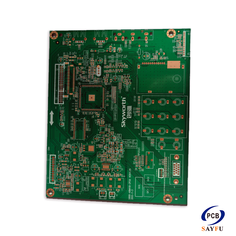
General Specification:
Layer count: 8 rank HDI board
Material: FR-4 Halogen Free
Finish thickness: 1.55 ±10%mm
Minimum width/spacing: 3.6/3.2mil
Minimum via diameter (laser blind via): 0.15mm
Specialty: L1-2,L7-8: laser drilling, 3 rank HDI, Laser blind vias:1-2,2-3;3-4
L8: characteristic impedance with 75 ohms ±10%
Differential impedance with 100 ohms ±10%
Surface finish: OSP
Application: telecom
This halogen-free 8-layer 3-rank HDI PCB is designed for telecom applications that need dense routing and controlled impedance in a 1.55 mm finished board. It uses halogen-free FR-4, laser blind vias, OSP surface finish, 3.6/3.2 mil line width and spacing, and a 0.15 mm laser-via diameter.
The HDI build-up uses laser drilling between L1-L2 and L7-L8, with blind-via connections across L1-L2, L2-L3, and L3-L4. This structure creates routing space close to the outer layers without increasing the overall board outline. The stack-up and impedance requirements need to be included in the design package from the start.
Product Overview
The board carries 75 ohm single-ended impedance with a +/-10% tolerance and 100 ohm differential impedance with the same tolerance. These values are part of the electrical definition, not a generic material claim. Trace geometry, layer assignment, and the final stack-up need to remain aligned with the impedance target throughout the design.
Halogen-free FR-4 is specified for this product. When material selection is a project requirement, include the required laminate details and documentation expectations with the RFQ. This avoids treating a material requirement as a note added after the HDI structure has already been selected. Related multilayer and HDI context is available on the PCB manufacturing capabilities page.
HDI Build-Up and Routing
The laser blind vias and 3-rank construction make this board suitable for a compact telecom layout, but the via map must match the actual routing plan. Include the layer stack-up, impedance table, and drill information with the Gerber files. Where a controlled line changes layer, show the transition and reference-plane requirement in the design data.
The 3.6/3.2 mil routing is part of the product specification. Dense areas around BGA escape routing, connectors, and impedance-critical interfaces need sufficient clearance in the final layout. Send the relevant mechanical and assembly information when those areas have restricted placement.
Surface Finish and Production Information
OSP is specified for the exposed copper on this board. Pad design and assembly requirements should match the selected component and soldering process. If the project includes assembly, a component list, placement data, and assembly drawing provide the needed context; related support is described on the turnkey PCB assembly page.
What to Confirm Before Production
Please provide Gerber files, drill files, the HDI stack-up, and the impedance table. Include the layer-to-layer laser-via structure, finished thickness, OSP requirement, controlled-net details, quantity, and telecom application. This gives the quote a clear basis for reviewing the HDI build-up and electrical targets together.