10-Layer Stacked-Via HDI PCB with Immersion Gold
Images
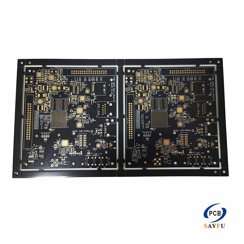
General Specification:
10L Stack vias HDI PCB
Layer count: 10 layer
Board thickness: FR4(tg150) 1.6mm
Minimum width/gap: 0.07/0.07mm
Minimum drill size: 0.1mm
Surface: immersion gold
Steps:1-2,2-9,9-10 Stack vias technology
Application: Military
This 10-layer stacked-via HDI PCB uses FR4 Tg150 at a 1.6 mm board thickness, 0.07/0.07 mm line width and spacing, 0.1 mm minimum drilling, and immersion gold. Its via structure includes L1-L2, L2-L9, and L9-L10 connections for dense routing across the outer and inner layers.
The stacked-via structure is relevant when the available board area cannot accommodate a conventional through-hole escape pattern. The via map, layer assignment, and component placement need to be developed as one layout. A stacked-via board cannot be quoted reliably from a board outline alone.
Product Overview
Ten layers provide room for signal, power, and reference layers in a compact HDI construction. The L2-L9 connection is a major part of the structure, so the required via sequence and routing intent need to be visible in the fabrication data. The 0.07 mm routing and 0.1 mm drilling dimensions also require the final Gerber and drill information rather than a general capability description.
FR4 Tg150 and immersion gold are specified for this board. Include the required finish and any interface-specific pad details in the RFQ. If a component footprint or connector places tight demands on the pad area, provide that drawing with the layout files.
Stacked Via Layout
Stacked vias create additional routing channels but add design dependencies between layers. Show the via spans, the layer stack-up, and any restricted routing zones in the production package. When a dense component field drives the HDI build-up, include the component drawing and placement information so the escape area can be reviewed in context.
The finished thickness is 1.6 mm. Mechanical mounting, connector height, and enclosure clearance still need to be checked against the full assembly. The HDI board dimensions alone do not define those requirements.
Applications and Assembly Fit
This product is identified for military applications. For any project using this board structure, the application-specific documentation, inspection expectation, and component requirements should be stated in the RFQ instead of assumed from the layer count. The PCB manufacturing capabilities page provides related board-fabrication context.
Where component installation is included, send the BOM, placement data, and assembly drawing with the PCB files. The turnkey PCB assembly page provides related assembly information.
What to Confirm Before Production
Please provide Gerber files, drill files, the 10-layer stack-up, and the stacked-via map. Include the L1-L2, L2-L9, and L9-L10 requirements, immersion-gold pad details, quantity, application, and inspection requirement. This lets the HDI structure and the final layout be reviewed together before fabrication.