2-Layer FR4 Hard Gold PCB with Flash Thick Hard Gold Finish
Images
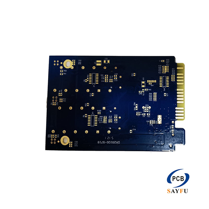
General Specification:
- Layer No: 2 layers
- Material: FR4 Tg150
- Board thickness: 1.0mm
- Surface finish:Flash thick hard gold(Min au 30u”)
- Min through hole: 0.3mm
- Min line width: 0.15mm
- Min line space: 0.2mm
- RoHS
This hard gold PCB is a 2-layer FR4 Tg150 board with a thin rigid structure, flash thick hard gold finish, controlled minimum feature sizes, and RoHS support. It is designed for projects where selected contact areas need better wear resistance than a standard solderable surface finish.
For buyers, the important value is the balance between simple 2-layer construction and a contact-capable finish. The board can support interface areas, contact pads, and selected conductive surfaces where the finish needs to be matched to the mechanical use of the final product.
Hard Gold Finish for Contact Areas
Hard gold is commonly selected for contact surfaces that may experience repeated insertion, sliding, or electrical contact. The minimum Au 30 uinch hard gold requirement should be reviewed against the expected product function and contact frequency.
The 2-layer structure keeps the board simpler than a multilayer design, while the 1.0 mm thickness supports products where mechanical space is limited. This makes the hard gold area and board outline especially important during design review.
Material and Feature Control
FR4 Tg150 provides a stable material base for this hard gold PCB. The listed minimum hole, line width, and line spacing values should be checked against the circuit layout before fabrication, especially around connector, contact, or test-point areas.
For related process support, see PCB manufacturing capabilities and the special process PCB category.
What to Confirm Before Production
Before production, confirm the hard gold area drawing, gold thickness requirement, solder mask clearance around contact areas, board thickness, hole data, RoHS requirement, and whether the contact edge needs any special mechanical treatment. These details help the manufacturer quote the correct finish instead of treating the board as a standard ENIG PCB.
Typical Applications
This hard gold PCB is suitable for contact pads, edge contacts, connector areas, switch contacts, test interfaces, and other designs where selected surfaces require improved wear resistance or reliable electrical contact.
Custom Hard Gold PCB Manufacturing
For quotation and manufacturability review, provide Gerber files, drill files, hard gold area drawing, gold thickness requirement, board thickness, material requirement, RoHS requirement, and expected production quantity. For design preparation questions, see the FAQ on design and technical issues.