14-Layer Multilayer PCB with ENIG and Controlled Impedance
Images
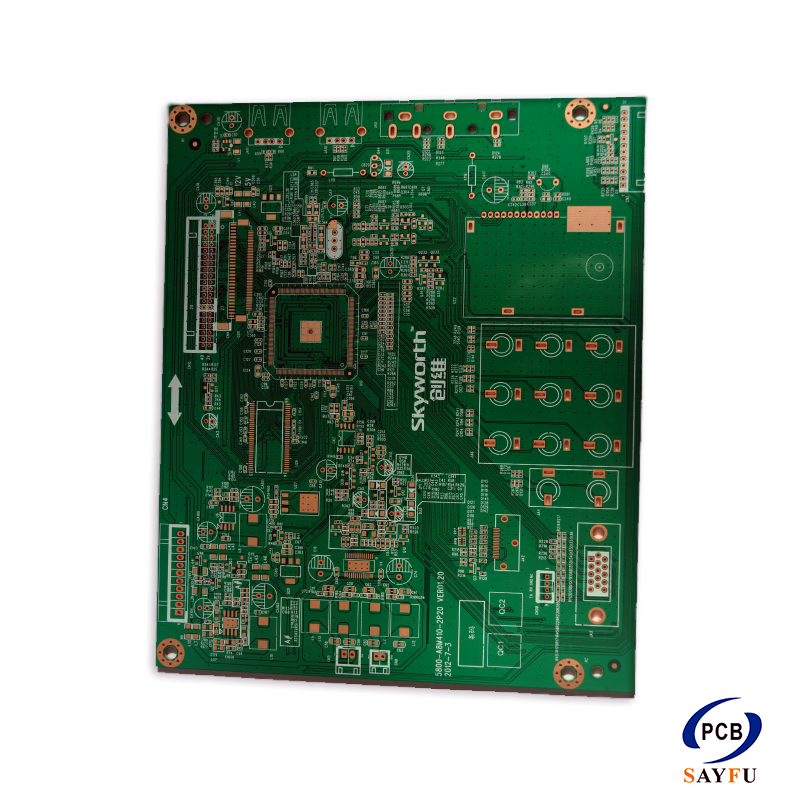
General Specification:
Layer count: 14
Finish thickness: 1.6±0.2mm
Minimum width/spacing:
Outer layer :4/5mil
Inner layer: 3.7/4mil
Minimum via diameter: 0.15mm
Surface finish: ENIG
Controlled impedance
Specialty: Inner via to line: 8mil;
Annular ring: 5mil;
Divider: 7.9mil
Application: Inverter, Transformer, Power Box, ECG, UAV etc
This product is a 14-layer multilayer PCB with ENIG finish, controlled impedance, fine outer and inner layer spacing, small via capability, and application references including inverter, transformer, power box, ECG, and UAV electronics. It is designed for projects that need high layer count routing in a standard finished board thickness range.
The board is suitable when routing density, reference plane planning, impedance behavior, and via reliability must be considered together. Specialty spacing and annular ring requirements should be reviewed with the full stack-up before quotation.
High-Layer-Count Routing Value
A 14-layer PCB gives designers more routing layers and reference planes for complex circuits. This helps support dense signal routing, power distribution, ground planning, and controlled impedance structures in a compact rigid board.
The finished thickness range keeps the board compatible with many mechanical designs, but building 14 layers into that thickness requires careful stack-up planning. Material, copper thickness, and dielectric spacing should be confirmed before production when impedance or reliability is important.
Fine Features, Vias, and ENIG Finish
The small via and fine line spacing requirements call for controlled drilling, imaging, etching, plating, and inspection. The difference between outer-layer and inner-layer spacing should be reviewed against the full stack-up and trace routing plan.
ENIG provides a flat solderable surface for assembly. For broader multilayer capability, see PCB manufacturing capabilities.
What to Confirm Before Production
Before production, confirm the stack-up, material grade, copper thickness, impedance values, via rules, annular ring requirements, surface finish, and final application environment. For power electronics, ECG, UAV, or inverter-related products, reliability expectations and operating conditions should be shared with the quotation files.
Typical Applications
This board is suitable for inverter, transformer, power box, ECG, UAV, industrial control, power electronics, and other products that need high layer count routing and controlled impedance.
Custom Multilayer PCB Manufacturing
For quotation and manufacturability review, provide Gerber files, drill files, stack-up drawing, impedance requirements, via requirements, line width and spacing rules, surface finish requirement, application notes, and expected production quantity. For file preparation questions, see the FAQ on design and technical issues.