Selective Hard Gold PCB for Gold Finger and Contact Areas
Images
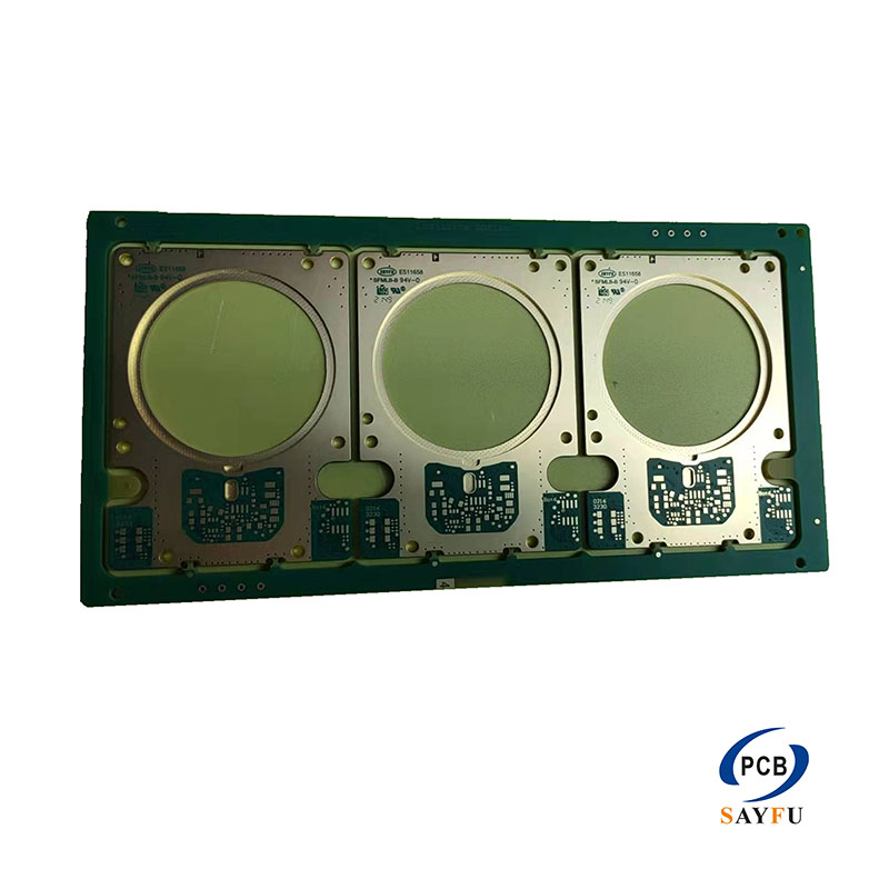
General Specification:
layer: 18
material: FR4 ITEQ
Board thickness: 3.0mm
Surface finish: Immersion Au+Selective thick hard gold(Min au 30u”)
Min through hole: 0.3mm
Min line width: 0.15mm
Min line space: 0.2mm
RoHS
Application: Military+
This product is a selective hard gold PCB for boards that need durable gold-plated contact areas, such as gold fingers, edge contacts, switch contacts, or test interfaces. Selective hard gold thickness up to 80 uinch can be considered when the contact area requires stronger wear resistance.
Selective hard gold is different from applying one finish across the whole board. It is usually placed only where wear resistance or repeated electrical contact is required, while other areas may use a solderable finish depending on the assembly design.
Selective Hard Gold Design Value
Hard gold can improve wear resistance on connector or contact areas, but the plated region must be clearly defined in the fabrication files. The customer should identify which pads or edges need hard gold, whether beveling is needed, and how the finished contact will be used.
For related special-process context, see the special process PCB category and PCB manufacturing capabilities.
Application Fit
Selective hard gold PCB is suitable for connector fingers, plug-in modules, key contact areas, test points, industrial control boards, and other products where a contact surface may see repeated insertion, friction, or measurement.
What to Confirm Before Production
Before production, confirm the hard gold area drawing, gold thickness requirement, nickel requirement if specified, bevel or edge requirement, solder mask clearance, surface finish for non-contact pads, and inspection expectations. This prevents the board from being quoted as a standard ENIG PCB when the product actually needs selective hard gold control.
Custom Selective Hard Gold PCB Manufacturing
For quotation and manufacturability review, provide Gerber files, drill files, and hard gold area drawing, gold thickness requirement, board thickness, finish requirement, bevel note if applicable, quantity, and contact-use background. For design preparation questions, see the FAQ on design and technical issues.