16-Layer Isola 370HR HDI PCB for Industrial Computers
Images
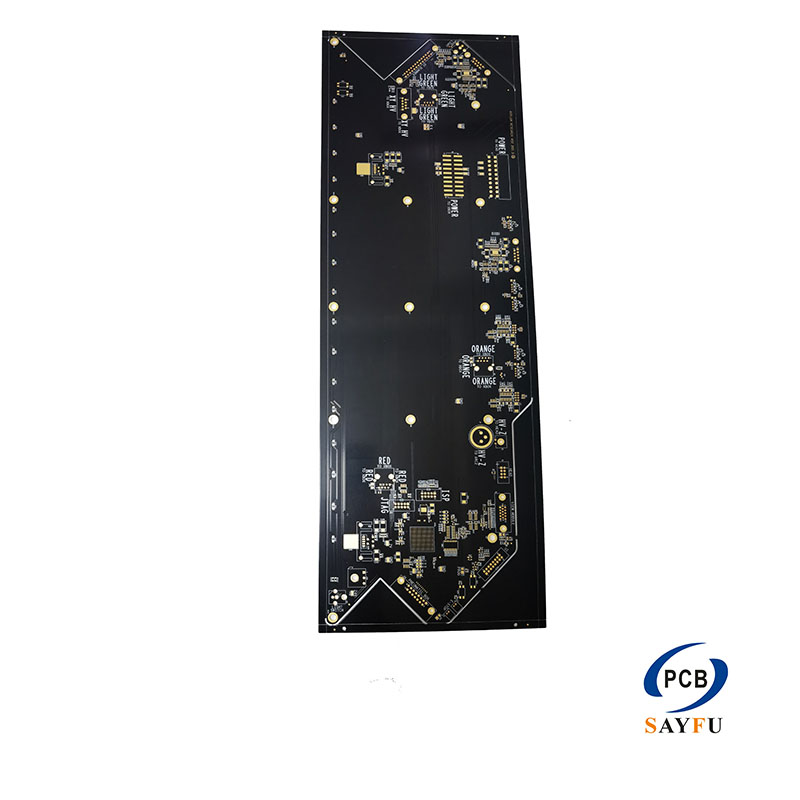
General Specification:
ISOLA Printed Circuit Board
Layer Count:16
The board thickness is 2.50mm
Material: ISOLA 370HR
The minimum drill hole is 0.15mm
Min line width and space is 0.15mm/0.15mm
Have blind vias: L1-L2, L1-L8, and L9-L16
Surface treatment: immersion silver
Application:Industrial Computer
This 16-layer Isola 370HR HDI PCB is specified for industrial computer applications. The board uses a 2.50 mm finished thickness, 0.15 mm minimum drill size, 0.15/0.15 mm line width and spacing, blind vias between L1-L2, L1-L8, and L9-L16, and immersion silver surface treatment.
The layer count and blind-via spans point to a dense multilayer design with routing requirements across both outer and inner sections of the stack-up. The material, via map, and routing plan need to be reviewed as one board definition. A 16-layer board cannot be quoted accurately from thickness and layer count alone.
Product Overview
Isola 370HR is the material identified for this construction. Include the requested material and any project-specific documentation requirement with the RFQ. The final stack-up should show the layer order, dielectric arrangement, copper requirements, and the intended blind-via spans.
The 2.50 mm profile also makes connector height, mounting hardware, and enclosure clearance relevant to the finished design. Provide the related mechanical drawing when those constraints affect board edges, mounting holes, or component placement.
Blind Vias and Dense Routing
The L1-L2, L1-L8, and L9-L16 blind-via requirements need to appear in the via map and fabrication notes. These spans create routing options, but they also affect layer planning and drill documentation. Include the completed Gerber files, drill data, and stack-up rather than describing the structure only in a purchase note.
The 0.15 mm line width, spacing, and drill size are specified for this product. Dense component areas, controlled nets, and layer transitions should be clear in the design files. State any impedance requirement with the relevant net or stack-up information.
Surface Finish and Application Fit
Immersion silver is specified for the exposed pads. The solder mask, pad geometry, assembly process, and handling requirements need to suit the final component set. If the board will be supplied with assembly, include the BOM, placement data, and assembly drawing; related support is described on the turnkey PCB assembly page.
This board is identified for industrial computers. Include the required application, mechanical constraints, and inspection expectation with the RFQ. The PCB manufacturing capabilities page provides additional context for multilayer HDI projects.
What to Confirm Before Production
Please provide Gerber files, drill files, the 16-layer stack-up, and the blind-via map. Include the Isola 370HR requirement, immersion-silver pad details, finished thickness, quantity, application, and inspection requirement. This provides a clear basis for reviewing the material, HDI structure, and final layout together.