4-Layer Aluminum MCPCB for LED Lighting
Images
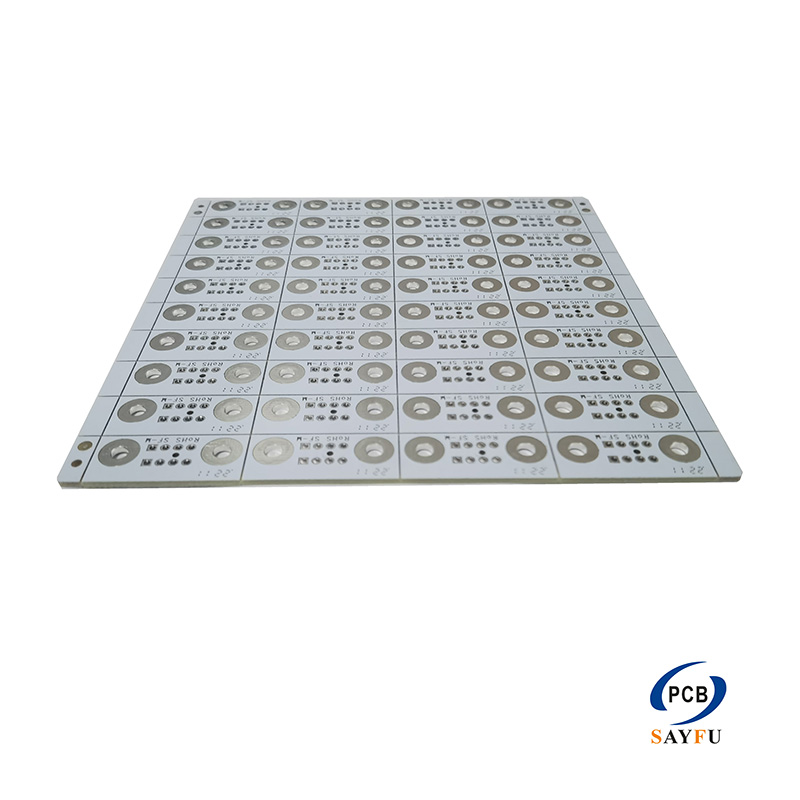
General Specification:
Material: Totking(Aluminum Based)
Layer:4L
Board Thickness:1.5mm
Copper thickness:1OZ
Soler Mask:Black&white
Thermal conductivity:3.0 w/m.k
This 4-layer aluminum MCPCB is specified for LED lighting with Totking aluminum-based material, 1 oz copper, a 1.5 mm board thickness, black and white solder mask, and stated thermal conductivity of 3.0 W/m.K. It is intended for a lighting design that needs multilayer routing together with a metal-backed construction.
Four layers provide more routing options than a conventional single-layer aluminum PCB. They can accommodate a more involved connection pattern, but the stack-up, via structure, and component layout need to be defined in the design package. The layer count alone does not show how the LED circuit, control lines, or power connections are arranged.
Product Overview
The Totking aluminum-based material and stated 3.0 W/m.K thermal conductivity are specific to this product. They should not be presented as a general value for every MCPCB. A project with a different power level, dielectric structure, or thermal target needs its own material requirement and stack-up.
The 1.5 mm profile also forms part of the mechanical design. When the board mounts inside a lamp body, reflector, channel, or heat sink, include the mating-surface drawing and fixing method with the RFQ. Mounting holes, board edges, optical clearances, and connector access all need to agree with the finished assembly.
Multilayer Routing and Vias
A four-layer MCPCB needs clear fabrication data for the internal connections. The Gerber files, drill data, and stack-up should identify the layer sequence and required interconnections. If the design includes controlled nets or specific reference layers, add those requirements to the stack-up rather than relying on a general multilayer note.
The 1 oz copper specification needs to be retained in the board data. Final conductor widths and clearances should follow the actual LED and control circuit. Tight areas around connectors, drivers, and component pads are best reviewed from the completed layout and footprint information.
LED Assembly Fit
Black and white solder mask are specified for this product. The artwork should identify which areas use each color and keep the mask definition consistent with the LED layout. Pad geometry, mask openings, polarity marks, and component orientation need to match the selected LED package and soldering process.
For projects supplied with LEDs, drivers, connectors, or other components, provide the BOM, placement data, and assembly drawing with the fabrication files. Related support is described on the turnkey PCB assembly page.
LED Lighting Applications
This board is intended for LED lighting products that need a multilayer connection pattern on an aluminum-based structure. It may fit compact lighting modules where the PCB carries LEDs together with additional routing, provided the material, thermal interface, and mechanical outline match the final product.
If the design includes an LED array together with driver or control components, identify the functional areas in the assembly drawing. This gives the multilayer routing useful context and shows which component groups, connectors, and mounting features control the board outline. It also distinguishes the LED-side mask artwork when black and white solder mask are both required.
Separate artwork files may be needed when the color areas vary by product version.
For a quotation, provide Gerber files, drill files, the four-layer stack-up, and the mechanical outline. Include the Totking material requirement, solder-mask color definition, LED layout, quantity, application, and inspection requirements. Related construction options appear on PCB manufacturing capabilities.