2-Layer Heavy-Copper Aluminum PCB for LED and Power Designs
Images
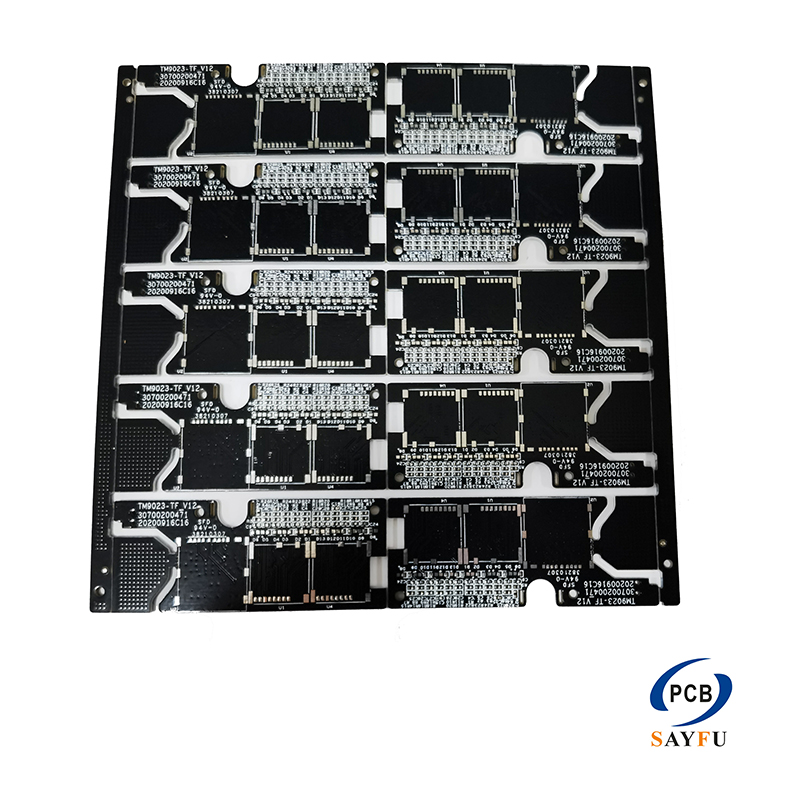
General Specification:
Aluminum base board (Aluminum PCB)
Detailed Product Description
Material: Aluminum
Board Thickness:1.6mm
Layer: 2
Copper thickness: 5OZ
Soler Mask: Black
Finish: HAL-LF
This 2-layer aluminum PCB uses a 1.6 mm board thickness, 5 oz copper, black solder mask, and lead-free HASL. The two-layer layout and heavy-copper construction are intended for LED or power-related circuits that need more routing freedom than a single-sided metal-core board can provide.
The 5 oz copper requirement needs to appear in the final stack and fabrication notes. It should also be reflected in the conductor layout, pad design, and connection method. The product data does not state a current rating, so the required current path needs to come from the customer's electrical design rather than a general assumption about heavy copper.
Product Overview
Two copper layers provide routing on both sides of the board. This can be useful when the component arrangement, power connections, or control routing cannot be completed cleanly on one side. The via and through-hole requirements need to be included in the drill data because they form part of the connection between the two copper layers.
The 1.6 mm board profile must fit the installed housing, heat sink, or mounting frame. Include mounting holes, edge clearances, connector positions, and any cutouts in the mechanical drawing. For a board installed against metal hardware, identify the required electrical clearance around fixing points and exposed conductors in the design files.
Heavy Copper Layout
Five-ounce copper changes the space available for routing and pads compared with a lighter copper design. Conductor widths, clearances, and copper distribution need to be shown in the completed Gerber files. Dense routing should not be inferred from the layer count alone, especially around power terminals, connectors, and component pads.
The copper layout also needs to account for the board outline and component footprint. If a connector or terminal carries the main current path, include its drawing and pad recommendation with the RFQ. This gives the connection area a defined geometry for review before fabrication.
Surface Finish and Assembly
Lead-free HASL is specified for exposed pads, with black solder mask over the protected copper areas. Pad size, solder-mask clearance, and hole dimensions need to match the selected components and soldering process. Black solder mask is part of the stated board construction and should be included in the fabrication notes.
For boards supplied with LEDs, connectors, power terminals, or other components, provide the BOM, placement data, and assembly drawing. The turnkey PCB assembly page provides related information for combined fabrication and assembly projects.
Application Fit
This structure can be considered for LED and power-related products that require two copper layers and 5 oz copper on an aluminum board. Suitability depends on the actual circuit, current path, component selection, and mechanical installation. Those details should be included when they affect copper geometry, board outline, or assembly requirements.
When the design includes several power connections, label the relevant terminals and conductor paths in the drawing package. Separate notes for the main current path, control circuit, and connector interfaces make it easier to relate the heavy-copper requirement to the actual layout.
This is particularly useful when several connector options share the same board outline.
For a quotation, provide Gerber files, drill files, the board outline, and current-path information. Include the 5 oz copper requirement, black solder mask, lead-free HASL pads, quantity, application, and inspection requirements. Further board context is available on PCB manufacturing capabilities.