Single-Sided Aluminum Core PCB with 3 oz Copper
Images
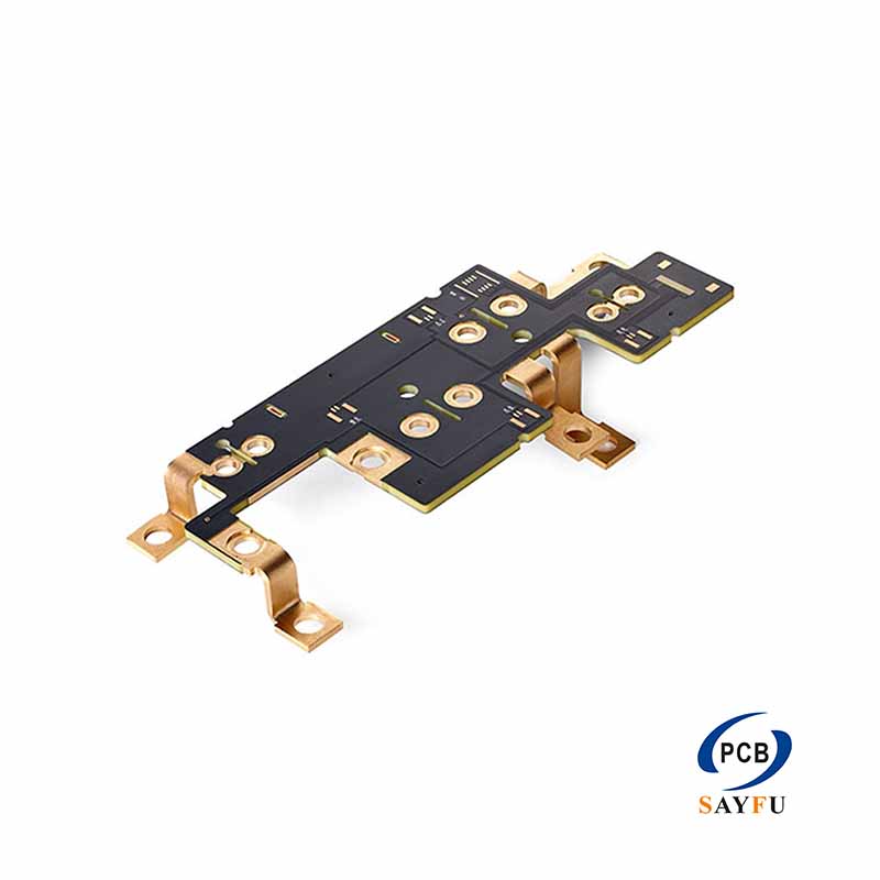
General Specification:
Single sided Metal core pcb
Finish thickness: 1.7±0.17mm
Minimum width: 0.54mm
Minimum via diameter: 3.175mm
Surface finish: HASL Lead Free
Aluminum core board
Copper thickness: 3oz
Aluminum core thickness: 1.5mm
Dielectric material: 80um
This single-sided aluminum core PCB uses 3 oz copper, a 1.5 mm aluminum core, 80 um dielectric material, lead-free HASL, and a 1.7 +/-0.17 mm finished thickness. It is intended for a simple one-layer circuit that needs heavier copper on a metal-backed board.
The 3 oz copper and aluminum-core construction need to be reflected in the current path, pad layout, and mechanical design. The product data does not state an application or current rating, so the electrical requirement should come from the completed circuit rather than a broad assumption about heavy copper.
Product Overview
A single-sided layout works when all required routing can be completed on one copper layer. The 0.54 mm minimum line width gives the stated routing feature for this product. Final conductor widths and spacing still need to follow the actual load, component layout, and clearance requirements in the Gerber files.
The board uses a 1.5 mm aluminum core and 80 um dielectric material within a finished thickness of 1.7 +/-0.17 mm. These dimensions matter where the PCB fits into a machined housing, mounting frame, or fixed connector position. Include the mating mechanical drawing when the thickness tolerance or board edge controls installation.
Hole and Mechanical Requirements
The minimum via diameter is specified as 3.175 mm, a relatively large feature that may relate to the connection or mechanical design of this product. The supplied drill data should identify the purpose of each hole rather than treating all holes as interchangeable. Mounting holes, terminal holes, slots, and cutouts need their finished dimensions in the mechanical drawing.
Board-edge clearance is also important on a metal-core construction. Copper and pads must follow the clearances defined by the actual design. If the board fastens to a metal surface, show the fixing points and any required clearance around exposed conductors.
Heavy Copper and Pad Design
Three-ounce copper affects the conductor and pad layout compared with a lighter copper board. The main current path, terminal positions, and copper distribution should be visible in the design package. When several connector or terminal options share one outline, identify the option being quoted and provide the corresponding footprint data.
Lead-free HASL is specified for the exposed pads. Pad geometry and soldering details need to match the selected component, terminal, or connector. For boards supplied with components, provide the BOM and assembly drawing; related information is available through turnkey PCB assembly.
Application Fit
This board can be considered for power, lighting, or other single-layer metal-core designs when 3 oz copper, the specified core construction, and the mechanical hole pattern suit the product. The customer application and current-path information are needed to judge that fit.
If the product uses more than one terminal arrangement, include the drawing for the option being quoted. Terminal size and location can change the pad pattern, large-hole requirements, copper distribution, and assembly method even when the finished board outline remains unchanged.
Where mounting hardware also changes, provide the corresponding mechanical drawing so the drill data and board-edge clearances remain tied to the correct assembly option.
For a quotation, send Gerber files, drill files, the board outline, and current-path information. Include the 3 oz copper, dielectric and core requirements, quantity, application, and inspection requirements. See PCB manufacturing capabilities for related board context.