8-Layer Mobile HDI PCB for Communication Applications
Images
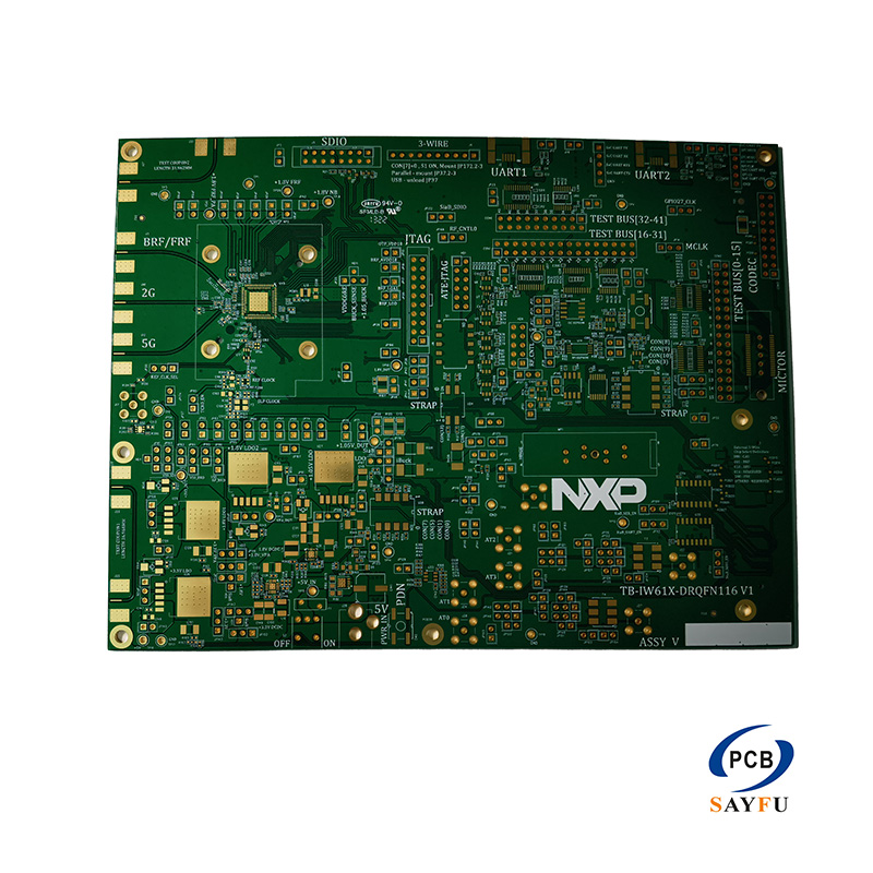
General Specification:
Mobile HDI PCB
Layer count: 8
Finish thickness: 1.0±0.1mm
Minimum width/spacing: 0.12/0.12mm
Laser blind: 0.127mm
PTH: 0.2mm
Application: Communication
This 8-layer mobile HDI PCB is specified for communication applications with a 1.0 +/-0.1 mm finished thickness, 0.12/0.12 mm line width and spacing, 0.127 mm laser blind vias, and 0.2 mm plated through-holes. The compact structure is intended for electronic layouts that need dense interconnects without adding excessive board thickness.
The laser blind vias and through-holes serve different routing roles. The blind-via design creates local routing space near the outer layers, while the plated through-holes connect the layers required by the final circuit. The stack-up and via map need to be included in the design package so the HDI structure can be evaluated against the actual component placement.
Product Overview
An 8-layer HDI board can separate signal, power, and reference layers in a compact communication product. The 1.0 mm profile makes mechanical clearance important. Include the enclosure, connector, and mounting constraints when the board fits close to a display, housing, battery, or other module.
The 0.12 mm routing dimensions and 0.127 mm laser blind vias are specified for this board, not general design targets. Dense routing areas should be taken from the finished Gerber files and component footprint data.
Via Structure and Layout
The component escape pattern, via spans, and layer transitions should be clear before quotation. Supply the HDI stack-up, drill table, and any controlled-net information with the PCB files. If a dense component field requires a specific placement sequence or restricted area, add the related drawing to the RFQ.
For communication electronics, the routing plan also needs to show which connections require special electrical treatment. Do not rely on the layer count alone to communicate impedance or reference-plane requirements; state them in the stack-up and net documentation.
Assembly and Application Fit
This board is intended for communication products. When the project includes mounted parts, connectors, or a defined assembly process, provide the BOM, placement data, and assembly drawing with the fabrication files. Related support is described on the turnkey PCB assembly page.
The PCB manufacturing capabilities page provides additional context for HDI and multilayer board projects. It should not replace the product-specific stack-up or via requirements in the RFQ.
What to Confirm Before Production
Please provide Gerber files, drill files, the HDI stack-up, and the laser-via map. Include the finished thickness, 0.127 mm laser-via requirement, 0.2 mm PTH requirement, routing constraints, quantity, communication application, and inspection expectation. This gives the quote a clear basis for reviewing the electrical and mechanical requirements together.