10-Layer FR4 TG170 Multilayer PCB with Resin Plugged Vias
Images
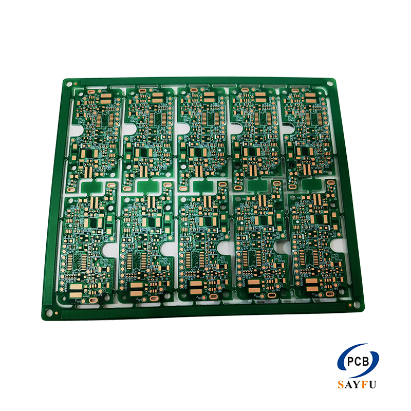
General Specification:
Layer No: 10 layer
Unit size/mm: 138mm*224mm
Panel size/mm: 95mm*121.5mm
trace width/space: 0.10mm/0.10mm
Material: FR4 TG170
Finished Thickess: 1.7mm
Finished Copper: 2/2…2/2oz
Surface treatment: ENIG
Soldermask: Green
Silkscreen: White
Profile Method: CNC Routing
Specialty: resin plugged for vias,2 cores have different copper foil in both sides
This product is a 10-layer FR4 TG170 multilayer PCB with ENIG finish, fine trace spacing, green solder mask, white silkscreen, CNC routing, resin plugged vias, and a 1.7 mm finished board thickness. It is suitable for designs that need more routing layers, stable mechanical structure, and controlled via treatment in a rigid multilayer PCB.
Different copper foil conditions on two cores mean the stack-up, copper balance, resin plugging, and routing requirements should be reviewed together before fabrication, because these factors affect lamination behavior and finished board flatness.
Multilayer Structure and Routing Value
A 10-layer PCB provides more routing and plane separation than a simple multilayer board. This is useful when the circuit needs signal layers, power layers, and ground reference layers in a controlled structure.
The board size and panelization requirements should be checked against the customer's production needs. The finished thickness gives the board mechanical stability while still supporting the multilayer stack and the via treatment required by the design.
Copper, ENIG, and Resin Plugged Vias
The fine trace width and spacing support dense routing for a 10-layer board. Copper balance should be confirmed with the stack-up because copper distribution can affect etching, lamination, and warpage.
Resin plugged vias can support smoother surfaces and more flexible routing when via locations must be controlled carefully. ENIG provides a flat solderable finish for assembly. For broader manufacturing support, see PCB manufacturing capabilities.
What to Confirm Before Production
Before production, confirm the stack-up drawing, copper distribution, resin plug locations, solder mask and silkscreen colors, surface finish, board outline, and panel requirements. If the product has assembly constraints, connector areas, or planarity requirements, those should be included with the quotation files.
Typical Applications
This board is suitable for compact multilayer electronics, control systems, communication circuits, power-related control modules, and products that require dense routing with a rigid multilayer structure.
Custom Multilayer PCB Manufacturing
For quotation and manufacturability review, provide Gerber files, drill files, stack-up drawing, copper thickness requirements, resin plugging notes, surface finish requirement, solder mask and silkscreen colors, board outline drawing, and expected production quantity. For file preparation questions, see the FAQ on design and technical issues.