10-Layer Rigid-Flex PCB with 4 Flex and 6 Rigid Layers
Images
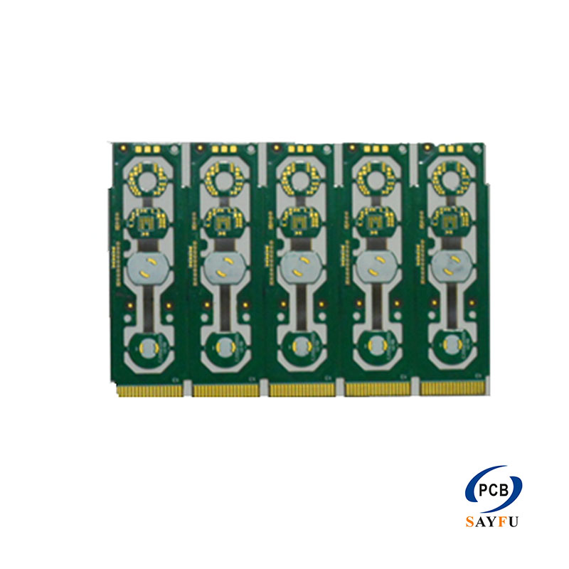
General Specification:
Layer count :4flex+ 6rigid;
Material : FR4+PI;
Copper thickness: 1/H/1/1/1/H/1..OZ
Board thickness: 0.3mm flex ,1.6mm rigid
0.25mm via,Green soldermask , white silkscreen
Trace width/space: 3.5/3.5mil
Surface finish: Immersion Gold
This 10-layer rigid-flex PCB combines four flex layers with six rigid layers in an FR4 and PI construction. The flexible section is specified at 0.3 mm and the rigid section at 1.6 mm, with 3.5/3.5 mil trace width and spacing, 0.25 mm vias, green solder mask, white silkscreen, and immersion gold.
The structure is intended for a compact product that needs substantial routing in both the rigid and flexible areas. Four flex layers provide more connection options than a simple two-layer flex, while the six rigid layers support component placement and internal routing. The complete layer arrangement needs to be shown in the rigid-flex stack-up.
Product Overview
The FR4 rigid sections and PI flex section form one integrated circuit. The design package should identify which copper layers continue through the flex, where rigid sections begin and end, and how the layers connect. A general ten-layer label does not provide enough detail for this construction.
The 0.3 mm flex thickness and 1.6 mm rigid thickness create distinct mechanical areas. Include the installed position of each rigid section, connector direction, flex length, and available enclosure space. This is particularly useful for products with several boards or modules connected inside a narrow housing.
Multilayer Flex Routing
Four flex layers give the design additional routing capacity, but they also make the flex stack-up and bend requirement more important. If the flex moves during operation, include the intended movement and bend information with the RFQ. The product data does not state a bend radius or cycle rating, so neither should be assumed.
The 3.5/3.5 mil routing and 0.25 mm vias are specified for this board. Dense component escape areas, via locations, and layer transitions need to appear in the completed Gerber and drill files. Any impedance requirement should be identified with the relevant net and layer reference information.
Rigid-Flex Transition and Materials
The transition between FR4 and PI needs a clear material definition in the stack-up. Show the coverlay, solder-mask, and pad-opening boundaries in the artwork. Connector or stiffener drawings should be included where they control the supported area at the end of a flex section.
The copper sequence is listed as 1/H/1/1/1/H/1.. oz in the available specification. Because that notation requires project-level interpretation, the final copper distribution should be confirmed in the stack-up before quotation. Use the approved stack-up as the controlling copper definition for the project.
Surface Finish and Assembly
Immersion gold is specified for exposed pads, with green solder mask and white silkscreen on the rigid areas. Pad geometry and openings need to match the selected components and connectors.
For an assembled rigid-flex PCB, provide the BOM, placement data, assembly drawing, and handling requirements for the flex sections. Related information is available through turnkey PCB assembly.
Applications
Rigid-flex boards of this type can be used in compact electronic products such as mobile devices, controls, computers, displays, storage equipment, and other assemblies that need several rigid areas connected by flexible circuitry. The final application, not the category name alone, determines the stack-up and mechanical fit.
For a quotation, provide Gerber files, drill files, the complete rigid-flex stack-up, and the installed mechanical drawing. Include the flex path, connector data, quantity, application, and inspection requirements. Related rigid-flex context is available on PCB manufacturing capabilities.