PBGA IC Substrate for Plastic Ball Grid Array Package Designs
Images
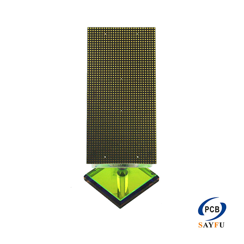
General Specification:
Number of layers: 4 layers (mainly), there are also designs with more than 6 layers
Structural features: There are many through-hole structures, the middle layer is mostly a copper layer, resin (main) or solder mask
Size: 1717mm~37.537.5mm
Board thickness: 0.4~0.6mm
Line width/line distance: 30/30 ~ 60/60 um
Gold finger spacing: 100~140 um
Surface treatment: Soft Au \ ENEPIG
Special process: TLP
PBGA IC substrate is used for plastic ball grid array package designs that need high I/O density, stable electrical connection, and package-level heat dissipation. This product is mainly a 4-layer PBGA substrate, with options for designs above 6 layers, 30/30-60/60 um line width and spacing, 100-140 um gold finger spacing, Soft Au or ENEPIG surface treatment, and TLP process support.
PBGA is a polymer plastic ball grid array package substrate. Compared with QFP and other pin-package forms, PBGA gives the chip package more I/O connection points in a compact area, so the substrate has to support both dense routing and reliable solder ball connection.
Why PBGA Substrate Parameters Matter
The 4-layer structure is suitable when a package needs more routing flexibility than a simple substrate but does not require the complexity of a very high-layer-count package board. If the package has a higher pin count or a more demanding ball map, designs above 6 layers may also be used.
The 17 x 17 mm to 37.5 x 37.5 mm package size range and 0.4-0.6 mm board thickness place this product in a compact package substrate category. At this scale, the buyer should confirm the ball grid layout, package outline, and available routing area before treating the board as a standard PCB order.
Routing, Finish, and Package Fit
The 30/30-60/60 um routing range supports fine interconnects for PBGA applications. This matters when the package has dense I/O and the routing must move signals from the ball grid to internal layers without creating avoidable clearance or registration problems.
Surface finish should be selected around the actual package connection requirement. Soft Au or ENEPIG can be relevant when the package needs stable contact quality, but the final selection should match the assembly process, reliability target, and customer drawings.
For related package-board capability, see IC substrate PCB capabilities and the IC substrates product category.
What to Confirm Before Production
Before quoting a PBGA substrate, the package drawing should show the ball map, substrate outline, layer requirement, and any special process notes. The middle-layer copper structure, through-hole design, resin or solder mask requirement, gold finger spacing, and TLP process should be checked against the intended package assembly.
If the design is for a higher I/O device, confirm whether a 4-layer build is enough or whether a structure above 6 layers is needed. This decision affects routing space, layer planning, cost, and manufacturing lead time.
Typical Applications
PBGA substrates are suitable for PC chipsets, ASICs, DSPs, memory devices, microprocessors, controllers, and graphics processors. They are a practical fit when the device needs more package I/O than pin-style packages can comfortably support.
Custom PBGA IC Substrate Manufacturing
SAYFU can manufacture PBGA IC substrates from customer package files and substrate design requirements. For quotation, provide package drawings and substrate design files, Gerber data if available, layer structure, package size, ball map, routing requirements, surface finish selection, TLP process notes, reliability requirements, and expected production quantity. For design preparation questions, see the FAQ on design and technical issues.