10-Layer FR4 TG210 Gold Finger PCB for Medical Applications
Images
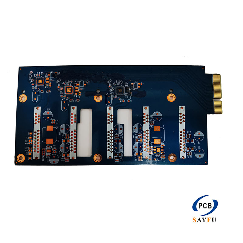
General Specification:
Material: FR-4 TG210
Layer: 10 layer
Thickness of cooper: 2/2 Oz
Thickness of board: 1.6MM
Surface finish: ENIG + Gold finger(AU 50U’)
Min. hole size: 0.15mm
Min.line width: 0.1mm
Min.line space: 0.15mm
Application: Medical
This product is a 10-layer FR4 TG210 gold finger PCB with heavier copper, ENIG plus gold finger finish, controlled small hole and trace features, and a medical application reference. It is suitable for designs that need reliable multilayer routing and durable contact areas for connector or interface use.
The combination of high Tg FR4 material, multilayer construction, 2 oz copper, and gold finger finish makes this board different from a standard prototype PCB. The contact area, plating thickness, board edge, and mechanical fit should be considered together when preparing files for quotation.
Gold Finger Contact Design
Gold fingers are used when the board edge or contact area must mate with a connector or interface. The Au 50 uinch gold finger requirement should be reviewed against insertion, contact stability, and product reliability requirements.
The 10-layer structure gives routing flexibility for complex circuits, while FR4 TG210 provides a high-Tg material base for applications where thermal stability is important. For medical electronics, the customer's reliability expectations and documentation needs should also be clarified before production.
Copper, Feature Size, and Contact Finish
The 2 oz copper should be considered together with trace width, spacing, current load, and etching control. The minimum line and hole requirements support compact routing, but they also require controlled fabrication and inspection.
For broader process capability, see PCB manufacturing capabilities and the special process PCB category.
What to Confirm Before Production
Before production, confirm the gold finger area drawing, plating thickness, bevel requirement if applicable, copper thickness, material requirement, connector fit, and any medical application expectations. These inputs help define the contact surface correctly and avoid treating the board as a normal ENIG multilayer PCB.
Typical Applications
This board is suitable for medical electronics, connector-edge interfaces, control boards, test interfaces, and multilayer designs requiring durable contact surfaces and stable PCB construction.
Custom Gold Finger PCB Manufacturing
For quotation and manufacturability review, provide Gerber files, drill files, gold finger area drawing, gold thickness requirement, bevel requirement if applicable, copper thickness, material requirement, medical application notes, and expected production quantity. For design preparation questions, see the FAQ on design and technical issues.