Peelable Mask PCB for Protecting Gold-Plated Contact Areas
Images
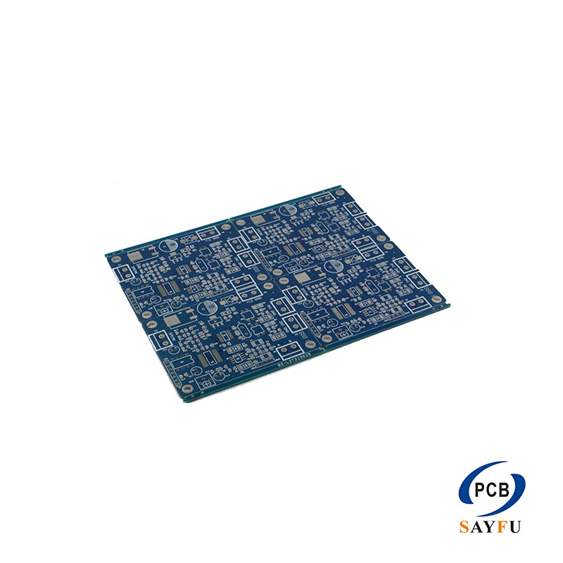
General Specification:
- Layer count: 6 layer
- Board thickness:1.6mm
- Raw material:FR4 S1000-2M
- Min.line width/space:4/4MIL
- Minimum hole diameter:0.10mm
- Surface finishing:HASL-LF
- Special item:Peelable
Peelable mask PCB is a 6-layer FR4 circuit board designed for applications where selected areas need temporary protection during fabrication, soldering, handling, or assembly. This board uses FR4 S1000-2M material, 1.6 mm finished thickness, 4/4 mil minimum line width and spacing, 0.10 mm minimum hole diameter, HASL-LF surface finish, and a peelable mask process for protected areas.
The peelable mask is used when certain pads, contact areas, or gold-plated regions must stay clean until a later production or assembly step. It acts as a removable protective layer, helping reduce contamination, solder exposure, oxidation risk, and handling damage on selected functional areas of the PCB.
Why Peelable Mask Matters on This Board
On a 6-layer PCB with 4/4 mil routing and 0.10 mm minimum hole capability, the board layout can contain relatively dense circuit features and small connection areas. If selected contact pads or process-sensitive surfaces are exposed during assembly, they may be affected by solder, flux residue, fingerprints, or oxidation before the final product is used.
A peelable mask helps protect those areas during processing without permanently changing the PCB structure. After soldering, cleaning, or assembly handling is complete, the mask can be removed so the protected surface is ready for electrical contact, testing, or final assembly.
This is especially useful when the board includes contact pads, test points, connector areas, or gold-plated surfaces that need controlled protection during production.
PCB Construction and Surface Finish
This peelable mask board is built as a 6-layer FR4 PCB, giving the design more routing flexibility than a simple double-sided board. The 1.6 mm board thickness is a common finished thickness for rigid PCB applications where mechanical stability and standard assembly compatibility are required.
The FR4 S1000-2M material provides a stable base for multilayer PCB fabrication, while the 4/4 mil line width and spacing support tighter routing where the circuit layout requires more density. The 0.10 mm minimum hole diameter also makes this board suitable for designs with small vias or compact interconnect requirements.
The HASL-LF surface finish provides lead-free solderability for general PCB assembly. Because HASL-LF and peelable mask serve different functions, the protected regions should be clearly defined in the fabrication notes so the temporary mask does not interfere with solderable pads, inspection areas, or final contact surfaces.
Peelable Mask Process Control
The most important detail in a peelable mask PCB is not only that the process is used, but where it is applied. The protected area should be clearly marked in the Gerber files, fabrication drawing, or process notes.
Before production, the following points should be confirmed:
- Which pads, contact areas, or exposed surfaces require peelable mask protection
- Whether the mask edge has enough clearance from solder joints and component pads
- Whether the protected area must remain clean after soldering or handling
- Whether the mask removal step fits the customer's assembly process
- Whether the board requires any special packaging or handling after fabrication
SAYFU supports peelable mask PCB as part of its broader PCB manufacturing capabilities and special process PCB production.
Quality Control and Manufacturing Review
For peelable mask boards, production review should focus on both the standard PCB structure and the special protection process. The 6-layer stack-up, minimum trace spacing, minimum hole size, surface finish, and peelable mask area should all be checked together before fabrication.
Key manufacturing checks may include mask location, solder mask opening, routing clearance, drill data, layer registration, surface finish coverage, and final visual inspection of the protected area. If the protected region is connected to a functional contact surface, the inspection plan should confirm that the area remains clean and usable after the peelable mask is removed.
For design preparation questions, buyers can refer to the FAQ on design and technical issues.
Typical Applications
This peelable mask PCB is suitable for multilayer circuit boards where selected areas need temporary surface protection. Typical use cases include:
- Contact pads that should stay clean before final assembly
- Test points or programming pads used after soldering
- Connector contact areas exposed during handling
- Gold-plated or process-sensitive regions requiring temporary coverage
- Multilayer PCB projects with local protection requirements
The applications above indicate suitable use cases, but the final process should still be confirmed based on the customer's Gerber files, assembly flow, and protected-area requirements.
Custom Peelable Mask PCB Manufacturing
SAYFU can manufacture peelable mask PCB based on customer-supplied design files, fabrication notes, and process requirements. For this product type, the layer count, board thickness, FR4 material, minimum line width and spacing, minimum hole diameter, surface finish, and peelable mask area should be reviewed as one complete manufacturing requirement.
For quotation and manufacturability review, provide:
- Gerber files
- Drill files
- Stack-up or fabrication drawing
- Peelable mask location drawing or notes
- Surface finish requirement
- Assembly or handling notes if the protected area is process-sensitive
- Expected production quantity
Send your project files to confirm peelable mask PCB manufacturability and quotation.