8-Layer Ceramic HDI PCB for Industrial Control
Images
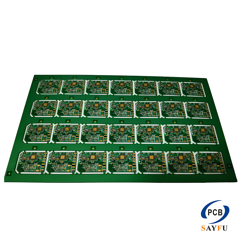
General Specification:
8 Layer HDI PCB for Industry control
Layer count:8
Materials: Ceramic
HDI 2+4+2 design, buried/blind via hole
Green LPI solder mask, white legend mark
PCB thickness: 2.0mm
Surface finish is ENIG (immersion gold)
Minimum trace/space: 0.1/0.1mm
Minimum hole: 0.1mm
This 8-layer ceramic HDI PCB uses a 2+4+2 build-up with blind and buried vias for industrial control applications. It has a 2.0 mm board thickness, green LPI solder mask, white legend, ENIG finish, 0.1/0.1 mm line width and spacing, and a 0.1 mm minimum hole size.
The 2+4+2 structure defines the HDI build-up, so the layer stack-up and via sequence need to be part of the quotation package. The board is not described by its layer count alone: the via locations, electrical routing, component density, and mechanical mounting requirements all need to agree with the final layout.
Product Overview
The ceramic HDI construction and 2.0 mm profile are specified for this product. Include the final material requirement and any application-specific constraints in the design data. A board material or thickness note without the stack-up and component information does not give enough context for an HDI quotation.
The 0.1 mm routing and hole dimensions support a dense layout. Send the completed Gerber and drill files for tight areas around components, connectors, and via transitions. This provides the geometry needed to review the actual board rather than a general quick-turn request.
HDI Structure and Assembly Fit
Blind and buried vias create routing space in an industrial control layout, but their spans and locations must be shown in the stack-up and drill documentation. If the board has impedance-critical nets, define the required impedance and layer reference information with the RFQ.
ENIG is specified for the exposed pads. Pad geometry, solder mask clearance, and component footprints need to match the intended assembly process. When components or connectors are included, supply the BOM, placement data, and assembly drawing. Related assembly support is available through turnkey PCB assembly.
Industrial Control Applications
This board is intended for industrial control. Include the operating environment, connector constraints, mounting arrangement, and inspection requirement when these items affect the product design. The PCB manufacturing capabilities page provides related HDI manufacturing context.
What to Confirm Before Production
Please provide Gerber files, drill files, the 2+4+2 stack-up, and the via map. Include the ceramic material requirement, ENIG pad details, finished thickness, routing constraints, quantity, application, and inspection expectation. This gives the production review a defined HDI structure and a usable set of manufacturing files.