6-Layer Rigid-Flex PCB with FR4 and PI
Images
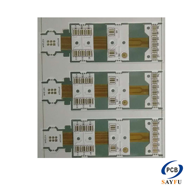
General Specification:
Layer No: 6 layer rigid-flex pcb
Panel size/mm: 110mm*92mm
Material: FR4 TG170&PI
Finished Thickess:1.6mm&0.2mm
Finished Copper: 35um
Surface treatment: ENIG
Soldermask: White
This 6-layer rigid-flex PCB combines FR4 Tg170 and PI, with a 1.6 mm rigid section, a 0.2 mm flex section, 35 um copper, ENIG, and white solder mask. The construction is suited to products that need component-supporting rigid areas and a defined flexible connection in one integrated circuit.
The rigid and flexible sections do different jobs. The FR4 areas support components, connectors, and mounting features, while the PI section routes the circuit through the product. Both areas need to be designed together because the flex path, rigid outline, and connector direction determine how the finished board fits the assembly.
Product Overview
Six layers provide routing space across the rigid-flex construction. The final stack-up needs to show which layers continue through the flex section and how the rigid sections connect. A general six-layer note is not enough for quotation because the material transitions and flex-layer arrangement are central to the product.
The rigid section is specified at 1.6 mm and the flex section at 0.2 mm. These thicknesses create two different mechanical conditions within the same board. Include the installed enclosure, mounting points, and connector locations when they control the flex length or the position of the rigid areas.
Flex Path and Transition Areas
The PI flex section needs a defined route between the rigid sections. The mechanical drawing should show the finished outline, bend direction, flex length, and any area that must remain free of components or hardware. If the flex moves during use rather than bending only during installation, state that operating condition with the quotation files.
The transition between rigid and flex areas deserves specific attention in the supplied data. Copper routing, coverlay openings, and the edge of the rigid construction need to follow the intended mechanical layout. Connector drawings and stiffener requirements should be included when they affect the termination area.
Copper, Finish, and Assembly
The board uses 35 um copper and ENIG on exposed pads. Pad geometry, coverlay or solder-mask openings, and component footprints need to match the planned assembly process. White solder mask is specified for the rigid areas and should be included in the fabrication artwork.
For an assembled rigid-flex board, provide the BOM, placement data, assembly drawing, and any handling restrictions related to the flex section. The turnkey PCB assembly page provides related information for projects that combine fabrication and component installation.
Application Fit
This construction is a practical option for compact equipment that needs several rigid mounting areas connected by a thin flex section. The application data should identify where the board is fixed, where it bends, and how connectors or components are accessed after installation. That information is more useful than a broad industry label when evaluating a rigid-flex design.
For products assembled in stages, include the installation sequence when it limits how the flex section can be folded or handled. A drawing of the installed position can clarify orientation between rigid sections and reduce ambiguity around connector direction, flex length, and available clearance.
This is also useful when more than one installation orientation is possible.
For a quotation, send Gerber files, drill files, the six-layer rigid-flex stack-up, and the mechanical drawing. Include the flex path, material sections, connector information, quantity, application, and inspection requirement. Related structure context is available on PCB manufacturing capabilities.