Single-Sided Flexible Circuit with PI Coverlay
Images
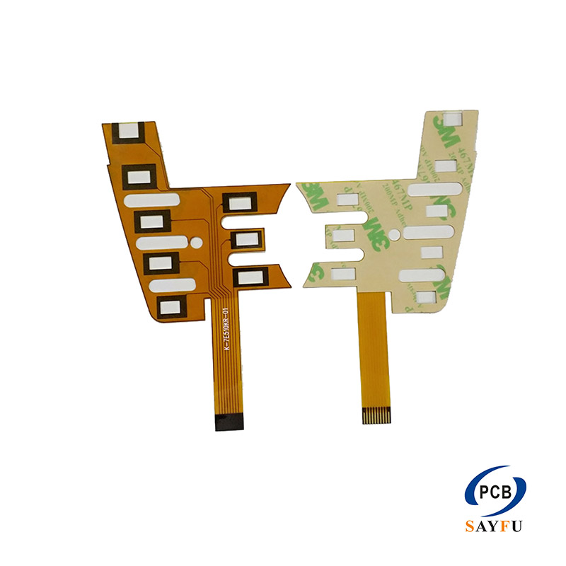
General Specification:
Layer No: 1 layer
Unit size/mm: /mm*/mm
Panel size/mm: 104mm*80mm
Material:FPC
Finished Thickess: 0.1-0.15mm
Finished Copper: ,1/Oz
Surface treatment:ENIG
Solder mask: PI Coverlay
Application: SWEEPER, pda,security control system, SW power
This single-sided flexible circuit uses one copper layer, a PI coverlay, ENIG surface treatment, and a finished thickness of 0.10-0.15 mm. It is designed for compact connections where the routing can be completed on one side of the circuit and the product benefits from a slim, flexible alternative to a rigid board or wire harness.
The circuit is a practical fit when the connection path is simple and the mechanical installation has already been defined. A one-layer FPC does not provide the same routing freedom as a double-sided or multilayer design, so pad order, connector direction, and the physical route through the product need to be considered before the outline is frozen.
Product Overview
The thin FPC construction can be used to connect separated modules without adding a bulky cable. Typical applications for this product include sweepers, PDA products, security control systems, and SW power applications. It can also be considered for other compact electronics that need a specific flexible connection and do not require a more complex multilayer route. Related structures are available through the FPC PCB product category.
The PI coverlay protects the circuit areas that are not intended to be exposed for soldering or connection. Its openings need to match the actual pad pattern and connector method. For a product with a narrow installation path, share the enclosure drawing or mechanical reference with the quotation files so the FPC outline can be reviewed against the installed position.
Routing and Bend Path
With one copper layer, a clean routing plan matters. A connection that looks simple on a flat drawing can become difficult to install when the flex has to turn around mounting features, pass a display, or reach a connector at a fixed angle. The bend path, pad locations, and connector orientation should be defined together rather than handed off as separate requirements.
Keep the bend area free of unnecessary pads, sharp copper corners, and sudden changes in route direction. When requesting a quote, include the bend path, connector position, coverlay openings, and any stiffener requirement in the production drawing. That allows the connection area to be reviewed before fabrication.
ENIG Pads and Assembly Fit
ENIG is specified for the exposed pads on this circuit. The pad geometry and coverlay opening need to suit the selected connector or soldering process. If the FPC will be supplied with components, connectors, or a defined assembly sequence, include those details in the RFQ. The turnkey PCB assembly page provides related information for projects that combine fabrication and assembly.
The 1 oz copper specification forms part of the circuit construction. The conductor width and spacing required for the final design should still be shown in the Gerber files. This is especially useful where the FPC connects to power-related electronics or has a tight pad pattern at the termination end.
What to Confirm Before Production
Please send Gerber files, drill files, FPC stack-up notes, and mechanical drawings with the requested quantity and application. Include the finished outline, bend requirement, PI coverlay details, ENIG pad locations, connector or stiffener drawings, and any inspection requirement. Clear files give the quotation a sound basis for reviewing the electrical connection and mechanical fit together.