Single-Sided FPC Circuit for LED Circuit Board Applications
Images
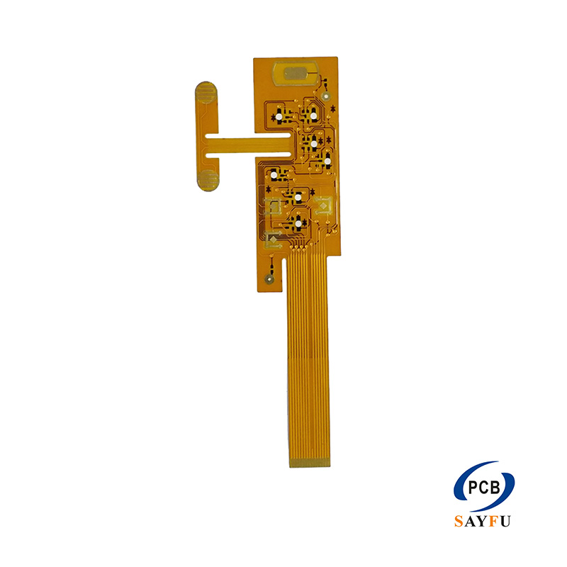
General Specification:
Material: PI, Copper thickness: 1oz; Standard board thickness: 0.13mm;
Min trace width/space: 4/4mil; Min hole size: 0.3m
Surface finish: ENIG
Application: CD-ROM pick-up; CDRW; LCD; Printer; LED light
This single-sided FPC circuit is made for compact connections in LED products and other electronics. It uses a PI base, 1 oz copper, a standard 0.13 mm finished thickness, and ENIG on the solderable areas. The one-layer construction suits jobs where a rigid PCB or wire harness would take up too much room.
Single-sided flex works best when the circuit can be routed without crossovers. The route, pad positions, connector direction, and bend path need to work together from the start. If the connection needs more routing freedom, it is worth reviewing the board construction before the layout is released. See the PCB manufacturing capabilities page for related flex options.
Product Overview
PI gives the circuit its flexible base and the copper layer carries the signal path. At 0.13 mm, the board can be used where a connection has to pass through a narrow enclosure, reach between two assemblies, or follow a set installation path. The mechanical layout matters as much as the electrical layout. The finished outline, folds, and connection points need to match the product enclosure before the fabrication files are released.
A simple flex circuit can save board space and remove a separate cable assembly, but only when the pad sequence and conductor routes are planned around the final installation. This is common in light modules, displays, control panels, and small electronic assemblies where the FPC has a defined path between the board and the connection point.
Routing and Interface Considerations
This design uses 4/4 mil trace width and spacing with a 0.3 mm minimum hole size. Those dimensions support a compact interconnect pattern, but they are not a substitute for checking the actual pad geometry, copper clearance, and termination method. A layout can pass an electrical review and still be difficult to build if the soldering areas or coverlay openings are too tight for the intended connection.
Keep the bend section clear of unnecessary pads, sharp copper corners, and sudden routing changes. When requesting a quote, include the connector position, solder pad support, coverlay openings, and any stiffener requirement in the production drawing. This allows the connection area to be reviewed before fabrication.
Surface Finish and Assembly Fit
ENIG is used on the exposed pads. For LED connections and compact assemblies, the pad size and coverlay opening must suit the selected component, connector, or soldering method. If the circuit needs a connector, reinforcement, or mounted component, show the location and orientation in the production drawing.
For a flex circuit supplied with components or connectors, discuss the assembly requirement before production. The turnkey PCB assembly page outlines the available support for projects that need fabrication and assembly together.
Applications
Typical uses include LED light products, LCD-related connections, CD-ROM pick-up units, CDRW products, and printers. It is also a practical choice for other compact electronics with a simple flexible connection. For an FPC that will bend in service, include the enclosure layout and intended bend path with the quotation files. This helps confirm that the outline, mounting points, and connector position suit the installed assembly.
What to Confirm Before Production
Please send Gerber files, drill files, and FPC stack-up notes, together with the quantity and application. Include the finished outline, bend-area requirement, coverlay details, ENIG pad locations, connector or stiffener drawings, and any inspection requirement. With that information, the routing, termination areas, and mechanical fit can be reviewed together before production.