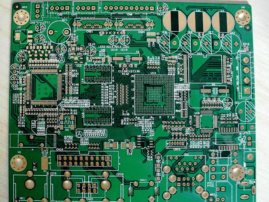
The Substrate-Like PCB (SLP) motherboard represents a significant technological evolution in the world of computing hardware. And primarily developed to meet the demands for thinner, lighter, and more powerful devices. Unlike traditional Printed Circuit Boards (PCBs), SLP technology utilizes manufacturing processes that are closer to those used in semiconductor packaging. This allowing for a much higher density of components and circuitry in a drastically smaller form factor.
The core advantage of SLP lies in its intricate design. It features extremely fine line widths and spacing, often measuring in microns. It is substantially smaller than what is achievable with standard PCB techniques. This miniaturization allows motherboard designers to pack more functionality—such as power delivery systems, memory modules, and intricate traces connecting the CPU, RAM, and storage—into a dramatically reduced space. Consequently, SLP is the foundational technology behind some of the most compact and sophisticated devices on the market, notably high-end laptops, ultrabooks, and 2-in-1 convertibles where internal real estate is at a premium.
For consumers, the benefits are immediately apparent. Devices built on SLP motherboards are remarkably slim and portable without sacrificing performance. This technology enables OEMs to create products with a nearly seamless, minimalist aesthetic while still incorporating powerful processors and fast memory. It is a key enabler of the modern trend toward “performance in portability.”
However, this innovation comes with trade-offs. The manufacturing complexity of SLP boards is exceptionally high, making them more expensive to produce than their standard PCB counterparts. This cost is often passed on to the consumer, positioning SLP-based devices in the premium segment of the market. Furthermore, the ultra-compact nature of these boards makes upgrades and repairs virtually impossible for end-users. As most components are soldered directly onto the board.
In conclusion, the SLP motherboard is a critical innovation driving the future of mobile computing. By pushing the boundaries of miniaturization and component density. It allows manufacturers to design the powerful, sleek, and portable devices that define the modern tech landscape. Even if it means embracing a more integrated and less user-repairable paradigm.