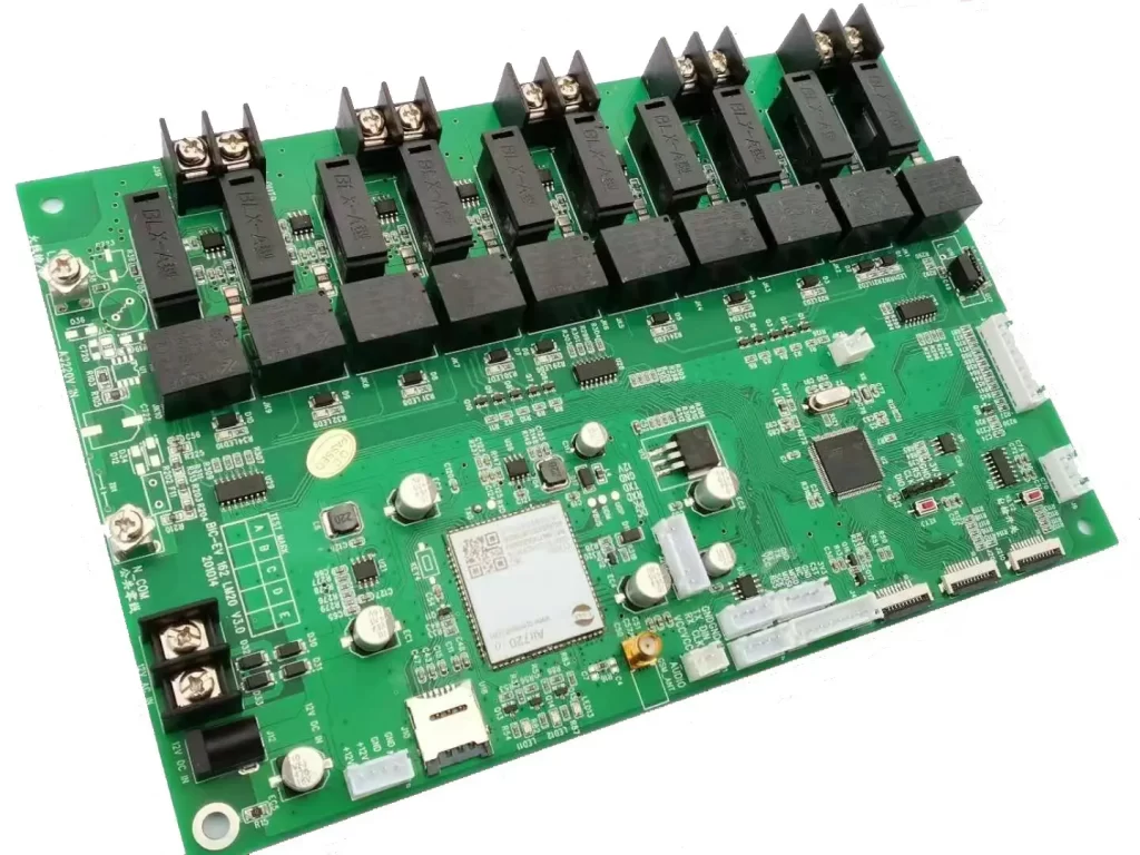
The Difference between ENIG and Hard Gold is quite an important thing for the PCB manufacturers all over the world. Because it is related to cost, durability and the PCB quality. PCB surface finish plays an important role on the PCB performance and its reliability. And among these treatment methods, ENIG and Hard Gold (or Gold Plating) are 2 commonly used methods. Below are the main differences for these 2 different treatment methods:
1. Process Principle Of ENIG and Hard Gold
1). Hard Gold (or Gold Plating). Electroplating gold is a process that deposits a nickel-gold alloy layer onto copper foil of PCB through electrochemical deposition. This process is to dissolve the gold salt (the mixture of nickel and gold) into the chemical potion. And then we immerse the circuit board in the electroplating tank and turn on the current. Thereby forming a plating layer on the copper foil surface. Gold plating, which is high hardness, wear-resistant and not prone to oxidation, is widely used in electronic products.
2). Immersion Gold (or Chemical Nickel Gold Plating). ENIG is a method of generating a plating layer on the PCB surface through chemical oxidation-reduction reactions. There is no the participation of currency. It is a process of depositing a nickel-gold layer on PCB PADs through chemical reactions. Usually, the Immersion Gold is a bit thicker, and it is a type of chemical nickel-gold layer deposition method.
2. The Coating Characteristics of ENIG and Hard Gold
1). Thickness and Color: Immersion Gold usually has thicker gold than that of Hard Gold. This makes the Immersion Gold surface finish has more golden color than that of Hard Gold in visual. Then we see the surface has a better visual effects.
2). Crystal Structure: Immersion Gold and Electroplated Gold have 2 totally different crystal structures. This results in differences in their physical and chemical properties. Such as, Immersion Gold finish is easier to solder than that of Hard Gold, and not prone to poor welding. However, Immersion Gold finish is softer than that of Hard Gold. Therefore, we usually use Hard Gold to produce gold finger PCB to improve the wear resistance of PCB.
3. The Performance and Applications
1). The Welding Performance. ENIG finish is more suitable for applications requiring high welding reliability. Due to its crystal structure being more conducive to welding. However, although Hard Gold has high hardness and better wear-resistant, it may not be as easy to solder as immersion gold.
2). Antioxidant Properties: Immersion Gold is not easier prone to oxidation with its more dense crystal structure, and by comparison. However, gold plating may be more prone to oxidation reactions in certain environments.
3). Short Circuits with Gold Wire. Line space and line width are getting more and more limited with the more and more layout dense. Gold plating in this situation is prone to causing gold wire short-circuit issues. However, gold sinking will not cause gold wire short circuits, because only the pads have a nickel-gold layer.
4). Solder Mask Over Bare Copper (SMOBC). For Immersion Gold finished PCB, there only has nickel-gold layer on PADs. This makes the solder mask on the circuit adhere more firmly to the copper layer, and when compensating, there almost has no influence on the space.
5). Flatness and Durability. Immersion Gold PCB usually has better flatness, and the durability is equivalent to that of gold-plated plates. All these give the Immersion Gold board an advantage in more demanding applications.
To sum up, Immersion Gold and electroplated gold treatments have their own characteristics and advantages in PCB surface treatment. The trade-off should be made based on specific application scenarios and requirements. For example, Immersion Gold may be more suitable for occasions requiring high welding reliability, strong oxidation resistance, minimal risk of gold wire short circuits and high good flatness requirements. While Hard Gold has more advantages than Immersion Gold for occasions requiring high hardness and wear resistance.
For most PCB manufacturers in China, especially for those manufacturers who can make Immersion Gold and Hard Gold treatments. Such as Sayfu and Sugar in Guangdong Province, when they come across a PCB case with gold finger. Only has Immersion Gold demands in the instructions, they usually need to check again with customers and ask them:
1. Do you need ENIG finish for the full plate?
2. Do you need Immersion Gold for PCB and Hard Gold for the gold fingers?