PCB design is an important link before PCB circuit board production. So, what is the PCB design process?
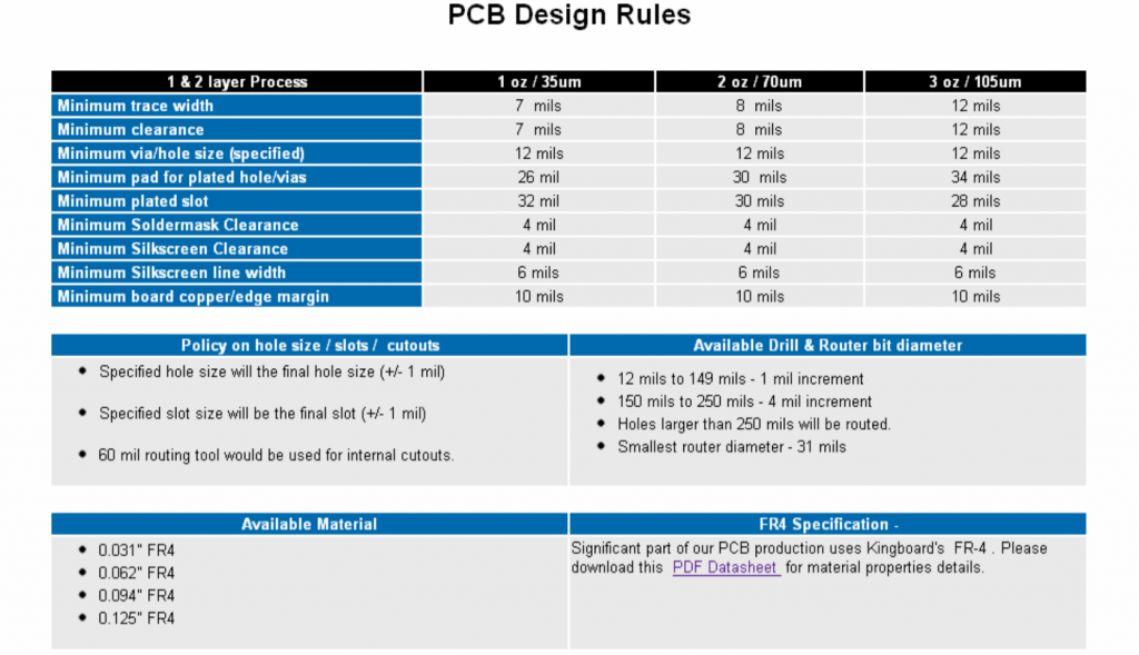
First: pre-preparation. Prepare component libraries and schematics. First, prepare the component library of the schematic SCH and the component library of the PCB. The component library can use the library that comes with peotel, it is best to make your own component library according to the standard size data of the selected device.
Second: PCB structure design. According to the determined circuit board size and various mechanical positioning, draw the PCB surface in the PCB design environment, and place the required connectors, buttons/switches, screw holes, assembly holes, etc. according to the positioning requirements.
Third: PCB layout. To put it bluntly, it is to put devices on the board. Generate a netlist on the schematic, and then import the netlist on the PCB diagram. The device can then be placed. The general layout is carried out according to the following principles:
- According to the reasonable division of electrical performance, it is generally divided into: digital circuit area, analog circuit area, and power drive area;
- Circuits that complete the same function should be placed as close as possible, and each component should be adjusted to ensure the most concise connection;
- For components with large mass, the installation position and installation strength should be considered; the heating element should be placed separately from the temperature sensitive element;
- The I/O drive device should be as close as possible to the edge of the printed board and the lead-out connector;
- The clock generator (such as: crystal oscillator or clock oscillator) should be as close as possible to the device that uses the clock;
- A decoupling capacitor needs to be added between the power input pin of each integrated circuit and the ground;
- A discharge diode should be added to the relay coil;
- The layout requirements should be balanced, dense and orderly, not top-heavy or heavy;
Fourth: wiring. Routing is the most important process in the entire PCB design. The wiring is mainly carried out according to the following principles:
- In general, the power line and ground wire should be wired first to ensure the electrical performance of the circuit board;
- Wire the lines with strict requirements (such as high-frequency lines) in advance, and the side lines of the input end and the output end should be avoided to be parallel to each other, so as to avoid reflection interference;
- The oscillator shell is grounded, the clock line should be as short as possible, and it should not be drawn everywhere;
- Use 45o folded line wiring as much as possible, and do not use 90o folded line to reduce the radiation of high-frequency signals;
- Do not form a loop in any signal line. If it is unavoidable, the loop should be as small as possible; the vias of the signal line should be as few as possible;
- The key lines should be as short and thick as possible, and protective ground should be added on both sides;
- When transmitting sensitive signals and noise field signals through flat cables, use the method of “ground wire-signal-ground wire”;
- Test points should be reserved for key signals to facilitate production and maintenance testing;
- After the schematic wiring is completed, the wiring should be optimized.
The above is the PCB design process. In a word, PCB design is a thought-provoking work, so you must be extremely careful when designing, fully consider all factors, and strive for excellence, you will be able to design a good board.