10-Layer 3-Rank HDI PCB with Immersion Gold Finish
Images
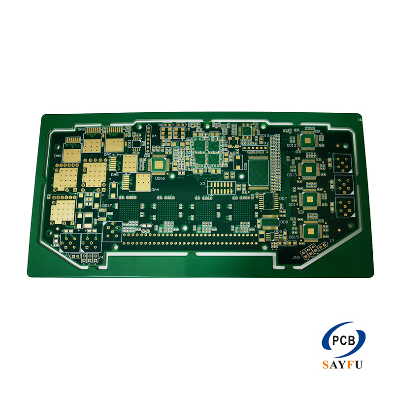
General Specification:
Layer No: 10 layers
Structure: 3 rank HDI, stacked vias, L1-2, L1-3, L1-4, L2-3, L2-4, L3-4, L4-7, L7-10, L7-8, L8-9, L7-9, L8-10, L9-10
Material: IT180A
Thickness: 1.6mm
Surface finished: Immersion Gold
Blind via L1-2 & L2-3 & L8-9 & L9-10: 0.1mm(4mil)
Buried via L4-8: 0.2mm(8mil)
Impedance control: differential 90 & 100ohm / 3 impedance control values
Minimum trace/space: 0.076mm/0.076mm
Green LPI solder mask and White legend mark
This product is a 10-layer 3-rank HDI PCB built with IT180A material, immersion gold finish, stacked via structures, blind and buried vias, fine trace spacing, and differential impedance control. It is intended for high-density designs where routing space, signal behavior, and via planning must be considered together.
Compared with a standard multilayer PCB, this board requires closer coordination between the stack-up, HDI build-up, impedance model, and assembly surface finish. The compact HDI structure must still be matched to the customer's circuit density, impedance target, and reliability environment.
HDI Structure and Routing Value
A 3-rank HDI structure allows more complex layer-to-layer interconnection than a standard through-hole multilayer board. Multiple stacked via paths across the stack-up help route dense IC areas while reducing dependence on through holes that consume routing space.
The blind and buried via structure is especially useful when the board has limited routing channels, high pin-count devices, or controlled impedance signals. For this kind of board, via reliability and layer registration should be discussed before release to production.
Material, Impedance, and Surface Finish
IT180A material supports multilayer construction where lamination stability and reliability are important. The finished thickness keeps the board compatible with many standard mechanical and assembly requirements while still carrying a complex 10-layer HDI stack.
The design includes differential impedance control, so trace geometry, dielectric spacing, copper thickness, and manufacturing tolerance should be reviewed as one system. This is more useful to the buyer than checking the impedance value alone, because the final result depends on the full stack-up.
Immersion gold provides a flat solderable finish for fine-pitch and high-density designs. For related process capability, see HDI PCB capability and the HDI board category.
What to Confirm Before Production
Before production, confirm the HDI stack-up, stacked via spans, impedance targets, material requirement, solder mask and legend requirements, and any automotive or high-reliability operating conditions. If the board is used in an automotive project, temperature range, vibration exposure, documentation needs, and validation expectations should be defined by the customer.
Typical Applications
This 10-layer HDI PCB is suitable for compact electronic products that need dense routing, controlled impedance, and multilayer interconnection. For automotive PCB use, final suitability should still be confirmed against operating temperature, vibration, reliability, and electrical requirements.
Custom HDI PCB Manufacturing
For quotation and manufacturability review, provide Gerber files, drill files, HDI stack-up drawing, impedance requirements, blind and buried via structure, material requirement, surface finish requirement, solder mask and legend requirements, and expected production quantity. For broader design preparation questions, see the FAQ on design and technical issues.