Get in touch

Factory address
Factory address: Yayao Town, Heshan City Jiangmen, Guangdong Province, China

Business office and transit warehouse address: 5th Floor, No.1 Buld, Dacheng jiancai Square, Guanchang Road, Dalingshan Town, Dongguan city, Guangdong Province, 523819
Phone number
+86 136 6295 5837

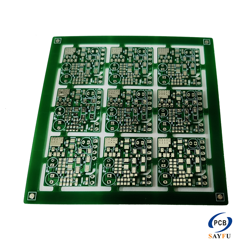
18-Layer Blind and Buried Via PCB for Telecom Applications

Images

Buried Via PCB,Backplane Circuits

General Specification: 

18-layer Multilayer Board

The board thickness of 3.02mm

Material: Isola FR408 special material

The minimum drill hole of 0.25mm

With buried and blind vias

Minimum line width and space of 0.10mm

Surface treatment: immersion gold

Controlled impedance: +/-10%

Application: Telecom

This product is an 18-layer blind and buried via PCB built with Isola FR408 special material, controlled impedance, immersion gold finish, fine line spacing, and a thick multilayer stack. It is suitable for telecom projects where routing density, signal integrity, and stable layer registration are usually central design concerns.

The value of this board comes from the combination of high layer count, blind and buried via structure, controlled impedance, and special material selection. These requirements make the product more demanding than a standard multilayer PCB because the via map, stack-up, and impedance model all affect the finished board.

Blind and Buried Via Structure

Blind and buried vias allow signals to move between selected layers without using only through holes across the full board. In an 18-layer PCB, this helps improve routing density and can free up surface routing space for complex circuits.

The minimum drill and fine line/space requirements should be reviewed together with the stack-up, routing density, and impedance needs before fabrication. This is especially important when telecom boards combine high layer count routing with controlled signal paths.

Material, Thickness, and Impedance

Isola FR408 is used as the special material for this board. Material selection matters in telecom applications where signal integrity, lamination stability, and predictable electrical behavior are important.

The 3.02 mm board thickness and 18-layer structure require careful lamination control. Controlled impedance tolerance of +/-10% should be supported through the stack-up, dielectric spacing, trace geometry, and manufacturing process.

For broader process capability, see PCB manufacturing capabilities and HDI PCB capability.

What to Confirm Before Production

Before production, confirm the stack-up, blind and buried via map, impedance values, material requirement, copper thickness, surface finish, board thickness tolerance, and telecom reliability expectations. These inputs help avoid quotation gaps when the product depends on both dense routing and controlled electrical performance.

Typical Applications

This board is suitable for telecom products, backplane circuits, high-layer-count routing, controlled-impedance designs, and complex multilayer electronics that require blind and buried via structures.

Custom Blind and Buried Via PCB Manufacturing

For quotation and manufacturability review, provide Gerber files, drill files, stack-up drawing, blind and buried via map, impedance requirements, material requirement, surface finish, application notes, and expected production quantity. For design preparation questions, see the FAQ on design and technical issues.