Get in touch

Factory address
Factory address: Yayao Town, Heshan City Jiangmen, Guangdong Province, China

Business office and transit warehouse address: 5th Floor, No.1 Buld, Dacheng jiancai Square, Guanchang Road, Dalingshan Town, Dongguan city, Guangdong Province, 523819
Phone number
+86 136 6295 5837

HDI PCB Manufacturing in China for High-Density Circuit Designs

Images
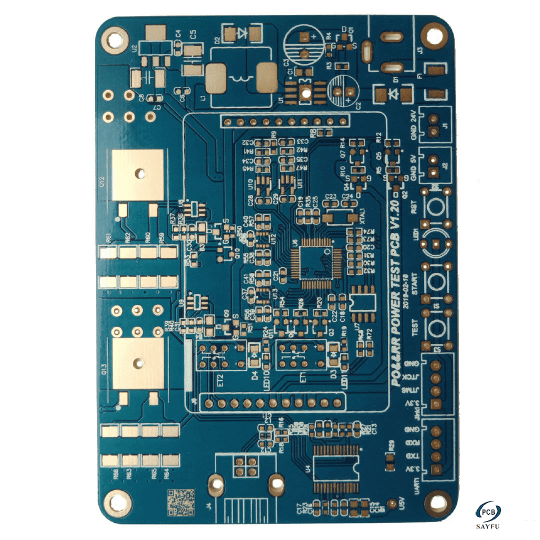
HDI PCB, pcb industry, pcb design

General Specification: 

  • Layer No: 8 layer
  • Panel size/mm: 101.85mm*132.36mm
  • Material: FR4 IT-180A
  • Finished Thickess:1.6mm
  • Finished Copper: 70um
  • Surface treatment: ENIG
  • Soldermask: Green
  • Soldermask: BLUE
  • Silkscreen: White
  • Special Technology:Buried Blind vias /resin plugged

HDI PCB manufacturing is used for high-density circuit designs where ordinary multilayer PCB routing cannot provide enough space for compact components, fine interconnects, and complex signal paths. This product is an 8-layer 2-rank HDI PCB built with FR4 IT-180A material, 1.6 mm finished thickness, 70 um finished copper, ENIG surface finish, white silkscreen, and buried blind vias with resin plugging.

The board size is 101.85 mm x 132.36 mm, making it suitable for compact electronic assemblies that require controlled routing density and stable multilayer construction. For buyers, the key value of this HDI PCB is not only the layer count, but the combination of 8-layer structure, HDI via technology, resin plugging, ENIG finish, and thicker finished copper for a more demanding circuit design.

Why 8-Layer HDI Construction Matters

An 8-layer HDI PCB gives designers more routing space than a standard 2-layer or 4-layer board while keeping the final board size controlled. This is important when the layout includes dense IC packages, limited board area, and signal routes that need shorter interconnect paths.

The 2-rank HDI structure with buried blind vias helps move signals between layers without relying only on through holes. Resin plugged vias also help improve surface planarity and routing flexibility, which is useful when component density is high or when pads, vias, and traces are placed close together.

This type of structure should be reviewed early in the design stage because HDI build-up, via placement, resin plugging, copper thickness, and layer registration all affect manufacturability.

Material, Copper, and Surface Finish

This HDI PCB uses FR4 IT-180A material with 1.6 mm finished thickness. FR4 IT-180A is suitable for multilayer PCB construction where stable lamination and reliable board performance are required. The 1.6 mm finished thickness also keeps the board compatible with many standard assembly and enclosure requirements.

The 70 um finished copper supports stronger current carrying than thinner copper designs and should be considered together with trace width, thermal behavior, and spacing rules. For an HDI design, copper thickness affects etching control, plating uniformity, and the available routing space.

ENIG surface finish provides a flat solderable surface, which is especially important for HDI boards with dense components, fine pads, and buried blind via structures. Compared with uneven surface finishes, ENIG is better suited for high-density assembly areas where solder joint consistency matters.

HDI Via and Resin Plugged Process Control

The buried blind vias and resin plugged process are central to this product. These features allow the board to support denser routing while maintaining a cleaner surface for later fabrication and assembly steps.

Before production, the via structure should be checked together with the stack-up, drill files, resin plugging requirements, and copper plating plan. If the HDI build-up is not clearly defined, the design may require CAM changes before fabrication.

Key manufacturing points include:

  • Whether the 2-rank HDI build-up is clearly shown in the stack-up
  • Whether buried and blind via locations match the routing strategy
  • Whether resin plugged vias are required under pads or in dense routing areas
  • Whether 70 um finished copper affects spacing and etching control
  • Whether ENIG is required for fine-pitch assembly or high-density pads
  • Whether the final solder mask color should be confirmed before production

SAYFU supports HDI production through its HDI PCB capability and related HDI board manufacturing range.

Quality Control and Manufacturing Review

For this HDI PCB, manufacturing review should focus on layer registration, lamination stability, buried blind via reliability, resin filling quality, copper plating, and final surface finish. The combination of 8 layers, 70 um finished copper, ENIG, and resin plugged HDI vias requires tighter process control than a standard multilayer board.

Gerber files, drill files, stack-up notes, impedance requirements, solder mask information, and via plugging requirements should be reviewed together before fabrication starts. If the board is used in a compact or high-reliability product, inspection requirements should also be confirmed before quotation.

For broader factory capability, see PCB manufacturing capabilities.

Typical Applications

This 8-layer HDI PCB is suitable for electronic products that need compact routing, high interconnect density, and reliable multilayer construction. Typical application directions include:

  • Communication modules and compact control boards
  • High-density consumer electronics
  • Industrial control hardware with limited board space
  • Products using dense IC packages or fine-pitch components
  • Multilayer PCB designs requiring buried blind vias
  • Designs that need ENIG finish for flatter solderable pads

The application fit still depends on the customer's circuit layout, operating environment, electrical requirements, and assembly process.

Custom HDI PCB Manufacturing

SAYFU can manufacture HDI PCB based on customer-supplied design files, stack-up requirements, via structure, material selection, copper thickness, surface finish, and production quantity. For this product type, the 8-layer structure, FR4 IT-180A material, 1.6 mm thickness, 70 um copper, ENIG finish, and buried blind via resin plugged process should be reviewed as one complete manufacturing requirement.

For quotation and manufacturability review, provide:

  • Gerber files
  • Drill files
  • HDI stack-up drawing
  • Buried and blind via structure
  • Resin plugging requirements
  • Copper thickness requirement
  • Surface finish requirement
  • Solder mask and silkscreen color confirmation
  • Impedance or reliability requirements if applicable
  • Expected production quantity

Send your project files to confirm HDI PCB manufacturability and quotation. For file preparation questions, see the FAQ on design and technical issues.