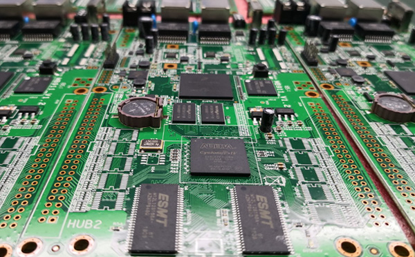
Modern communication technology is rapidly advancing for High-Frequency and High-Speed PCB: The Technological Artery Connecting the Future. Fields such as 5G, radar, and satellite communications demand increasingly higher performance in signal transmission. High-frequency and high-speed PCB serve as the core foundation enabling these technologies.
What are high-frequency and high-speed PCB?
They are specifically designed to handle high-frequency signals and fast data streams. Traditional circuit boards cannot meet such requirements. These advanced PCB effectively reduce signal loss and ensure the integrity and stability of information transmission.
Why is signal integrity so important for high-frequency and high-speed PCB?
In high-frequency environments, signals are prone to distortion, delay, or interference. Even minor errors can degrade system performance or cause failure. Therefore, PCB must possess excellent electrical properties and material characteristics.
Materials are key for high-frequency and high-speed PCB.
Conventional PCB substrates (e.g., FR-4) are unsuitable for high-frequency applications. Their high dielectric loss causes significant signal attenuation. In contrast, specialized materials (such as laminates produced by Rogers and Taconic) offer low dielectric constants, low loss factors, and outstanding thermal stability. These materials minimize energy loss during signal transmission.
Design and manufacturing are equally critical
PCB traces require precision design—they are no longer simple wires but accurately calculated transmission lines. Parameters like width, spacing, and dielectric thickness must be strictly controlled. Vias and copper surface treatments also need optimization to reduce reflection and noise.
Applications are broad and crucial.
From 5G base stations to self-driving cars, from military radar to satellite communications, high-frequency and high-speed PCBs are everywhere. Though hidden inside devices, they determine the performance and reliability of entire systems.
Looking ahead, with the advancement of IoT, AI, and 6G technology, high-frequency and high-speed PCBs will play an even more vital role. They are not only the backbone of the electronics industry but also an invisible bridge leading to an intelligent world, paving the way for tomorrow’s innovations.