PCB Design Basics Printed circuit boards (PCBs) appear in almost every electronic device. If there are electronic parts in a device, they are all mounted on PCBs of various sizes. In addition to fixing various small parts, the main function of the PCB is to provide the mutual electrical connection of the various parts above. As electronic devices become more and more complex, more and more parts are required, and the lines and parts on the PCB are also more and more dense.
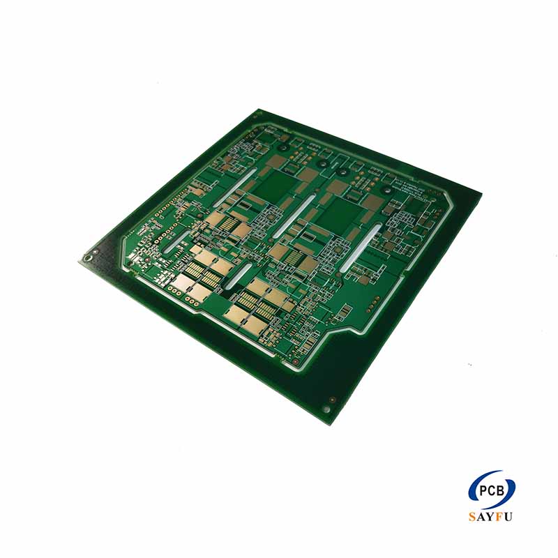
The bare board (with no parts on it) is also often referred to as a “Printed Wiring Board (PWB)”. The base plate of the board itself is made of insulating material that is not easily bendable. The thin circuit material that can be seen on the surface is copper foil. Originally, the copper foil covered the entire board, but part of it was etched away during the manufacturing process, and the remaining part became a mesh-like thin circuit. These lines are called conductor patterns or wiring, and are used to provide electrical connections to components on the PCB. To attach the parts to the PCB, we solder their pins directly to the wiring. On the most basic PCB (single-sided), the parts are concentrated on one side and the wires are concentrated on the other side. As a result, we need to make holes in the board so that the pins can pass through the board to the other side, so the pins of the part are soldered on the other side. Because of this, the front and back sides of the PCB are called the Component Side and the Solder Side, respectively.
If there are some parts on the PCB that need to be removed or put back after the production is completed, the sockets will be used when the parts are installed. Since the socket is directly welded to the board, the parts can be disassembled and assembled arbitrarily. Seen below is the ZIF (Zero Insertion Force) socket, which allows parts (in this case, the CPU) to be easily inserted into the socket and removed. A retaining bar next to the socket to hold the part in place after you insert it. If two PCBs are to be connected to each other, we generally use edge connectors commonly known as “gold fingers”. The gold fingers contain many exposed copper pads, which are actually part of the PCB layout. Usually, when connecting, we insert the gold fingers on one of the PCBs into the appropriate slots on the other PCB (usually called expansion slots). In the computer, such as graphics card, sound card or other similar interface cards, are connected to the motherboard by gold fingers. Green or brown on the PCB is the color of the solder mask. This layer is an insulating shield that protects the copper wires and also prevents parts from being soldered to the wrong place. An additional layer of silk screen is printed on the solder mask. Usually, text and symbols (mostly white) are printed on this to indicate the position of each part on the board. The screen printing side is also called the legend side.
Single-Sided PCB design
We just mentioned that on the most basic PCB, the parts are concentrated on one side and the wires are concentrated on the other side. Because the wires only appear on one side, we call this kind of PCB a single-sided (Single-sided). Because the single board has many strict restrictions on the design of the circuit (because there is only one side, the wiring cannot cross and must go around a separate path), so only early circuits used this type of board. Double-Sided Boards These boards have wiring on both sides. However, to use two sides of the wire, there must be a proper circuit connection between the two sides. Such “bridges” between circuits are called vias. Vias are small holes on a PCB, filled or painted with metal, that can be connected to wires on both sides.Because the area of the double-sided board is twice as large as that of the single-sided board, and because the wiring can be interleaved (can be wound to the other side), it is more suitable for use on more complex circuits than single-sided boards. Multi-Layer Boards In order to increase the area that can be wired, multi-layer boards use more single or double-sided wiring boards. Multi-layer boards use several double-sided boards, and put an insulating layer between each board and then glue (press-fit). The number of layers of the board represents several independent wiring layers, usually the number of layers is even, and includes the outermost two layers. Most motherboards are 4 to 8-layer structures, but technically, nearly 100-layer PCB boards can be achieved. Most large supercomputers use fairly multi-layer motherboards, but because such computers can be replaced by clusters of many ordinary computers, ultra-multi-layer boards have gradually fallen out of use. Because the layers in a PCB are so tightly bound, it’s generally not easy to see the actual number, but if you look closely at the motherboard, you might be able to.
The vias we just mentioned, if applied to double-sided boards, must be pierced through the entire board. However, in a multilayer board, if you only want to connect some of these traces, then vias may waste some trace space on other layers. Buried vias and blind vias technology can avoid this problem because they penetrate only a few of the layers. Blind vias connect several layers of internal PCBs to surface PCBs without penetrating the entire board.Buried vias are only connected to the inner PCB, so they cannot be seen from the surface. In a multi-layer PCB, the entire layer is directly connected to the ground wire and the power supply. So we classify each layer as signal layer (Signal), power layer (Power) or ground layer (Ground).
If the parts on the PCB require different power supplies, usually such PCBs will have more than two layers of power and wires. Component packaging technology Plug-in packaging technology (Through Hole Technology) The components are placed on one side of the board and the pins are soldered on the other side. This technology is called “Through Hole Technology (THT)” packaging. Such a part would take up a lot of space and would require drilling a hole for each pin. So their pins actually take up space on both sides, and the solder joints are relatively large. But on the other hand, THT parts and SMT (Surface Mounted Technology, Surface Mounted) parts, compared with the structure of the PCB connection is better, we will talk about this later. Sockets such as cables, and similar interfaces need to be able to withstand pressure, so usually they are THT packages. Surface Mounted Technology (Surface Mounted Technology) Using Surface Mounted Technology (SMT) components, the pins are soldered on the same side as the components. This technique eliminates the need for soldering for each pin, but instead drills holes in the PCB. Surface mount parts can even be soldered on both sides. SMT also has smaller parts than THT. Compared with the PCB using THT parts, the parts on the PCB using SMT technology are much denser. SMT package parts are also cheaper than THT ones. Therefore, it is not surprising that most of today’s PCBs are SMT. Because the solder joints and the pins of the parts are very small, it is very difficult to use manual soldering. But if you consider that the current assembly is fully automatic, most of this problem will only appear when repairing parts.
Design process In PCB design, in fact, before the formal wiring, there are still very long steps. The following is the main design process: System Specifications First, plan out the system specifications of the electronic equipment. Contains system features, cost constraints, size, operating conditions, and more. System functional block diagram Next, a functional block diagram of the system must be produced. Relationships between blocks must also be marked. Divide the system into several PCBs Dividing the system into several PCBs can not only reduce the size, but also allow the system to have the ability to upgrade and exchange parts. The system function block diagram provides the basis for our segmentation. For example, a computer can be divided into a motherboard, a graphics card, a sound card, a floppy drive, a power supply, and so on. Decide on the packaging method and the size of each PCB When the technology and the number of circuits used in each PCB are determined, the next step is to determine the size of the board. If the design is too large, then the packaging technology will be changed, or re-segmented. When choosing a technology, the quality and speed of the roadmap should also be taken into consideration.
Draw a schematic diagram of all the PCB circuits, and the schematic diagram should show the interconnection details between the various parts. PCBs in all systems must be described, and CAD (Computer Aided Design) methods are mostly used today. The circuit diagram of the PCB The simulation operation of the preliminary design In order to ensure that the designed circuit diagram can work normally, it must be simulated with computer software first. This type of software can read blueprints and display the circuit’s operation in many ways. This is much more efficient than actually making a sample PCB and measuring it by hand. Placing parts on the PCB The way parts are placed is determined by how they are connected to each other. They must be connected to the path in the most efficient way possible. The so-called efficient wiring is that the shorter the wire and the fewer layers that pass through (which also reduces the number of vias), the better, but we will mention this issue again when we are actually wiring. In order for each part to have perfect wiring, the placement position is very important. Test wiring possibilities and correct operation at high speed Some of today’s computer software can check whether the position of each component can be connected correctly, or whether it can operate correctly at high speed. This step is called arranging parts, and if there is a problem with the circuit design, it is possible to rearrange the position of the parts before exporting the circuit in the field. Exporting the wiring on the PCB The connections in the schematic will now look like the actual wiring.
The final picture of the PCB is usually called the work negative (Artwork). Every time a design is made, a set of rules must be met, such as the minimum reserved space between lines, the minimum line width, and other similar practical constraints. These regulations vary according to the speed of the circuit, the strength of the transmitted signal, the sensitivity of the circuit to power consumption and noise, and the quality of materials and manufacturing equipment. If the amperage increases, the thickness of the wire must also increase. In order to reduce the cost of PCB, while reducing the number of layers, it is also necessary to pay attention to whether these regulations are still complied with. If a structure with more than 2 layers is required, the power layer and the ground layer are usually used to avoid the transmission signal on the signal layer from being affected, and can be used as a shield for the signal layer. Behind-the-wire circuit testing To be certain that the circuit will function properly behind the wire, it must pass a final test. This test also checks for incorrect connections, and all connections follow the outline.
Creating a Fabrication File Because there are many CAD tools for designing PCBs, manufacturers must have a standard-compliant file in order to fabricate a board. There are several standard formats, but the Gerber files format is the most commonly used. A set of Gerber files includes floor plans for each signal, power, and ground plane, floor plans for solder mask and stencil printing, and specific files for drilling and pick and place.
Electromagnetic Compatibility Issues Electronic devices that are not designed according to EMC (Electromagnetic Compatibility) specifications are likely to emit electromagnetic energy and interfere with nearby electrical appliances. EMC sets maximum limits for electromagnetic interference (EMI), electromagnetic fields (EMF), and radio frequency interference (RFI). This regulation ensures the proper functioning of this appliance and other appliances nearby. EMC has strict limits on the energy that can be scattered or conducted to another device by one device, and is designed to reduce susceptibility to external EMF, EMI, RFI, etc. In other words, the purpose of this regulation is to prevent electromagnetic energy from entering or emitting from the device. This is actually a difficult problem to solve. Generally, power and ground layers are usually used, or the PCB is placed in a metal box to solve these problems. The power and ground layers can prevent interference on the signal layer, and the metal box is similar. We will not go too deep into these issues. The maximum speed of the circuit depends on how it is done according to the EMC regulations. Internal EMI, like current loss between conductors, increases with frequency. If the current gap between the two is too large, be sure to lengthen the distance between the two. This also tells us how to avoid high voltage and minimize the current consumption of the circuit. The delay rate of routing is also very important, so some high-speed PCB boards currently need to calculate timing.
Manufacturing Process The PCB manufacturing process starts with a “substrate” made of Glass Epoxy or similar material to begin the image (forming/wire making) The first step in the fabrication is to establish the wiring between the parts. We use Subtractive transfer to represent the working negative on the metal conductor. The trick is to spread a thin layer of copper foil over the entire surface and remove the excess. Additive Pattern transfer is another method that is less used, which is to apply copper wire only where it is needed, but we won’t talk about it here. If you are making a double-sided board, then the substrate of the PCB will be covered with copper foil on both sides. If you are making a multi-layer board, the next steps will glue the boards together. Positive photoresist is made from a photosensitive agent that dissolves under lighting (negative photoresist is one that breaks down without lighting). There are many ways to treat photoresist on a copper surface, but the most common is to heat it and roll it over a surface containing photoresist (called dry film photoresist). It can also be sprayed on in a liquid form, but the dry film type provides higher resolution and allows for thinner wires. The hood is just a template for the PCB layers in manufacturing. An overlying mask can prevent parts of the photoresist from being exposed (assuming a positive photoresist is used) before the photoresist on the PCB is exposed to UV light. These areas, covered by photoresist, will become wiring. After photoresist development, other bare copper portions to be etched. The etching process can be done by dipping the board in an etching solvent, or by spraying the solvent on the board. Commonly used as etching solvents are Ferric Chloride, Alkaline Ammonia, Sulfuric Acid + Hydrogen Peroxide, and Cupric Chloride. After the etching is completed, the remaining photoresist is removed. This is called the Stripping procedure. Drilling and Electroplating If a multi-layer PCB is made and contains buried or blind vias, each layer of the board must be drilled and electroplated before bonding. If you don’t go through this step, then there is no way to connect to each other. After drilling by machine equipment according to drilling requirements, the inside of the hole wall must be plated (Plated-Through-Hole technology, PTH). After the metal treatment is performed inside the hole wall, the internal layers of circuits can be connected to each other. Before starting electroplating, the debris in the hole must be cleaned. This is because the resin epoxy will undergo some chemical changes when heated, and it will cover the inner PCB layers, so it needs to be removed first. Both the cleaning and plating actions are done in the chemical process. Multilayer PCB Lamination The individual layers must be laminated to create a multi-layer board. The pressing action includes adding insulating layers between the layers and bonding them to each other.
If there are vias that pass through several layers, each layer must be processed repeatedly. The wiring on both sides of the outer side of the multi-layer board is usually processed after the multi-layer board is pressed. Handling Solder Mask, Screen Printing Surface and Gold Finger Partial Plating Next, apply solder mask paint to the outermost wiring so that the wiring does not touch the plated part. The silk screen printing surface is printed on it to indicate the position of each part. It cannot cover any wiring or gold fingers, otherwise it may reduce the solderability or the stability of the current connection. Gold fingers are usually plated with gold to ensure a high-quality electrical connection when inserted into the expansion slot. To test whether the PCB is short-circuited or open-circuited, optical or electronic tests can be used. Optical methods use scanning to find defects in each layer, while electronic testing typically uses a Flying-Probe to check all connections. Electronic testing is more accurate at finding shorts or opens, but optical testing can more easily detect problems with incorrect gaps between conductors. Parts Mounting and Welding The final step is to mount and weld the components. Both THT and SMT parts are installed and placed on the PCB using machine equipment. THT parts are usually soldered by a method called wave soldering. This allows all parts to be soldered to the PCB at once. First cut the pins close to the board and bend them slightly to allow the part to hold. Then move the PCB onto the co-solvent water wave, so that the bottom is in contact with the co-solvent, which can remove the oxide on the bottom metal. After heating the PCB, this time moving to the melted solder, after making contact with the bottom the soldering is done. The method of automatically soldering SMT parts is called Over Reflow Soldering. A paste-like solder that contains flux and solder, which is processed once after the part is mounted on the PCB, and once after the PCB is heated. After the PCB has cooled, the soldering is complete, and the next step is to prepare for the final test of the PCB. Methods to save manufacturing costs In order to keep the cost of the PCB as low as possible, there are many factors that must be taken into consideration: The size of the board is naturally an important point. . The smaller the board, the lower the cost. Part of the PCB size has become a standard, as long as the size is followed, the cost will naturally decrease. Using SMT will save space than THT because the parts on the PCB will be denser (and smaller). On the other hand, if the parts on the board are dense, the wiring must be thinner and the equipment used is relatively higher. At the same time, the materials used should also be more advanced, and the wire design must be more careful to avoid problems such as power consumption that will affect the circuit. The cost of these issues can outweigh the savings from shrinking the PCB size. The higher the number of layers, the higher the cost, but PCBs with fewer layers usually increase in size. Drilling takes time, so the fewer pilot holes the better. Buried vias are more expensive than vias that run through all layers. Because buried vias must be drilled before joining.
The size of the hole on the board is determined by the diameter of the pin of the part. If there are parts with different types of pins on the board, then because the machine cannot use the same drill to drill all the holes, it is relatively time-consuming, which also means that the manufacturing cost is relatively increased. Electronic testing using flying probe probing methods is generally more expensive than optical methods. Generally optical testing is enough to ensure that there are no errors on the PCB. All in all, manufacturers’ efforts in equipment are becoming more and more complex.
Understanding the manufacturing process of PCBs is useful, because when we are comparing PCBs, boards with the same performance may cost different and have different stability, which also allows us to compare the capabilities of various manufacturers. A good engineer can know the quality of the design just by looking at the PCB design.