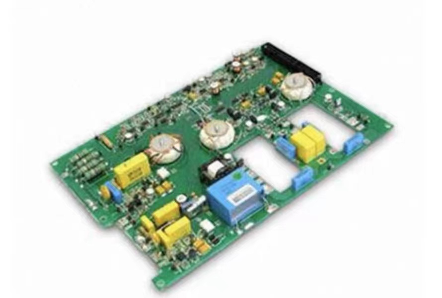
PCB Potion, we also call it the magic of electronic potting. In the intricate world of electronics manufacturing, reliability is paramount. Potting is one of the most crucial, yet often unseen, guardians process of this reliability. The material used for this—the PCB potion—is far from a magical brew. however, its protective qualities are indeed transformative for printed circuit boards (PCBs).
Section 1. Definition of PCB Potion
PCB (PrintedCircuitBoard), called printed circuit board for full name, is an important electronic components to support the main body of electronics product. It is also the provider of the electrical connection in the electronic components. Because we usually make it with electronic printing, we called it “printed” circuit board. The PCB board has the following three main types of classification:
PCBs refer to chemical products used in PCB manufacturing. Copper plate, copper foil, semi-curing tablets, chemical potion, anode copper/tin/nickel, dry film and ink, etc. Are all the main raw materials for PCB production.
Section 2. Development of PCB medicine industry.
The inventor of the PCB is Austrian Paul Esler, who use a PCB in radio installation in 1936. In 1943, americans used the technology heavily on military radios. The United States officially recognized the invention for commercial use since the mid-1950s, the PCB was widely used since 1948.
But before the printed circuit board appeared, direct wires make the interconnection between electronic components possible. Now, the circuit panel is only available as an effective experimental tool; Printed circuit boards have dominated the electronics industry. And PCB potion also came into being with the invention of printed circuit board.
Rigorous and scientific research methods can ensure the accuracy and quality of research reports. Potion “2012-2016 China PCB industry research depth and investment value study report” mainly adopts the research methods are:
1). Census. We PCB potion nearly hundred practitioners in the industry for the interview or telephone access, get the best data.
2). Tracking Research. In order to ensure the real-time dynamic potions master PCB industry. We have established tracking the potion in the PCB industry mechanism. And by accessing each month for PCB potions industry development.
3). Government Agency Data. We have inquired about the industrial and commercial files of key enterprises in PCB medicine industry, statistics bureau records, customs import and export data, etc. And obtained more authoritative information.
4). SOWT Analysis. By using SWOT analysis and porter’s five forces analysis. We analyzed the competitive advantages and potential threats and development opportunities of PCB potion industry and enterprises.
5). Scientific Prediction. We use regression analysis, time series analysis, factor analysis and combinatorial analysis, etc to make a full forecast of the development trend of PCB potion.
The content of the website is quite limit. If you feel this report is interesting, we will provide you with more value-added services. For details, please contact us directly online: http://www.sayfu-multilayer-pcb.com/ 。